This thread has been locked.

If you have a related question, please click the "Ask a related question" button in the top right corner. The newly created question will be automatically linked to this question.

BQ24171: BQ24171 Consultation on debugging issues

Part Number: BQ24171
Hello, FAE of Texas Instruments
I have some debugging issues with BQ24171 that I would like to consult with
Q1:At the beginning of debugging, there was no output because I set the PGND and AGND corresponding to the typical application diagram separately. Later, I studied the specification and found that these two GNDs need to be connected together, so there was output. I would like to ask why the two GNDs in the typical application diagram are separate, but in reality, they need to be connected together to output?
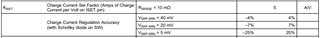
Q2:When I set the ISET voltage to 0.14V, the theoretical corresponding charging current should be 700mA (Rsr=10mΩ), but in reality, my charging current is 800mA, but the pre charging current is 166mA. What is the reason for this? Could you please help analyze it
  • Hi dxd,

    Regarding 1, I apologize.  I will submit for a datasheet update that shows PGND=AGND.  PGND has lots of switching noise current flowing from the converter.  Its common practice to route any components that need a less noisy ground away from PGND and then only connect PGND=AGND at the IC xGND pin if there are no separate PGND and AGND pins available.  If there were separate PGND and AGND pins, they would be connected inside the IC.

    Regarding 2, the current regulation loop is an analog feedback loop with specified accuracy, relative to the sensed voltage (and therefore value of the sense resistor)  below:

    With only 0.7A*0.01ohm = 0.007V sensed voltage, the accuracy is close to +/-25%.  Precharge and termination currents have the same, and slightly worse, problem.  If you need higher accuracy, you can increase Rsr, but will have slightly more losses which will lower efficiency.

    Regards,
    Jeff

  • HI,Jeff

    I'm glad to receive your reply. I still have some questions to inquire about

    Q1:Will the wiring of PGND and AGND affect current accuracy in PCBLayout? What is the better wiring method for PGND and AGND? I hope you can give me some suggestions

    Q2:Because the resistance value of Rsr can affect the current accuracy, my product outputs 2A, and the current accuracy needs to be ± 5%. Am I right to use a resistance of 0.02ohm for Vsrn srp to achieve 40mV?

    Q3:I found that the voltage accuracy of my DEMO is not very good when switching from fast charging to pre charging. I set the battery voltage to 0-3V to enter pre charging mode, but when the battery voltage is between 2.8-2.9V, the charging current will bounce back and forth between 2A and 200mA. What is the problem? Could you please help analyze it

    I hope to receive your prompt response to the above question. Thank you

  • Hi dxd,

    Regarding Q1, route all of the power pin (high current) capacitors on one side of the board and then the low current resistor grounds on the other side of the board.  The different grounds only connect close to the IC GND pin.

    Regarding Q2, yes.  40mV gives +/-4% accuracy.

    Regarding Q3, the charger is switching between precharge and fast charge.  That's no unexpected especially if the battery impedance is high.

    Regards,

    Jeff

  • Hi Jeff

    I'm glad to receive your reply. Please help me answer the following questions, thank you

    Q1:What is the principle of the diode connected between BTST and REGN in a typical application diagram? What is the rated voltage of the corresponding BTST? I couldn't find any relevant data in the specification book. Could you please help me answer it

    Q2:Is there a timer setting for Recharge, such as the 30min timer for Precharge. If so, how to set it up

    Q3:Is the cut-off current of the battery about to be fully charged the same algorithm as pre charging? When I actually debugged, the process of Trickle charging was very short, and the cut-off current was not very specific, so the charging ended. What is the reason for this?

    Q4:The Precharge I set is from 0-3V of the battery, but when my battery voltage is between 1-2V, the current will drop to around 20mA, which is a significant deviation from the 80mA I set. What is the reason for this?

  • Hi dxd,

    Regarding 1, BTST cap voltage = V(SW) = V(REGN) so a its the SW node referenced to V(REGN) not GND.  The boosted voltage is used for the gate driver of the high side FET.

    Regarding 2, no.  Recharge starts with the battery voltage drops below the VRCH threshold.

    Regarding 3, the device doesn't have trickle charge like our other parts.  It has a battery detection routine that injects 125mA as described on d/s page 20 section 9.3.15.

    Regarding 4, when below VBATSHT = 2V, the charger thinks the battery is shorted as behaves as explained below:

    9.3.16 Battery Short Protection When SRN pin voltage is lower than 2 V, it is considered as battery short condition during charging period. The charger will shut down immediately for 1 ms, then soft start back to the charging current the same as precharge current. This prevents high current may build in output inductor and cause inductor saturation when battery terminal is shorted during charging. The converter works in nonsynchronous mode during battery short.

    Regards,

    Jeff

  • Hi Jeff

    I'm glad to receive your reply. Please help me answer the following questions, thank you

    Q1:Can you please explain to me the principle and function of the diodes connected to the BTST and REGN pins in the typical application diagram of 5V input? Can this diode be cancelled? Modified to add Schottky diodes from SW pin to PGND?

    Q2:My understanding is that there is no specific value for the cut-off current when fully charged, right? Can it still be set?

    Q3:If the battery voltage is below 2V, the chip will determine that the battery is short circuited and restart after 1mS. When I actually debugged, when the battery voltage was 2V-1V, the pre charge current changed from 80mA to 20mA, but did it fail to restart when it returned to 80mA? Pre charging is 0-3V, with 80mA during the 0-1V and 2-3V processes. Can you help analyze where the problem lies? How to avoid this problem?

    Q4:When not connected to the battery, is the output voltage equal to the set full charge voltage? Assuming I set 4.4V and measure the output voltage without connecting to the battery, it will also be 4.4V

  • Hi dxd,

    Regarding 1, a diode is required so that the low side of the BTST is at REGN.  That means the high side of the BTST is the input voltage + REGN and is high enough voltage to turn on the high side FET.  There is an internal diode from BTST The Schottky from SW pin to GND is for improving efficiency and clamping the 

    Regarding 2, the charger doesn't termination until V(FB) is at the correct voltage per the resistor divider and the charge current has reduced to ITERM per below:

    If you have a load connected in parallel with the battery, the charger can't distinguish between load current and battery current.

    Regarding 3, the charger short protection is a last resort and assumes that the battery pack protector, which usually opens at # of cells *2.8V, has not opened. So, why is your battery voltage so low?   How are you holding the voltage below 2V? Is there some other load in parallel with the battery? Can you provide an oscope plot of V(BAT) and I(BAT)?

    Regarding 4, if no battery is connected (or pack protector is open) and charge is enabled (and not disabled due to TS fault), I expect the charger output to look like below:

    unless the output capacitance is above the Cmax value computed above.  Then the output will be at the the battery regulation voltage.

    Regards,

    Jeff