This thread has been locked.

If you have a related question, please click the "Ask a related question" button in the top right corner. The newly created question will be automatically linked to this question.

TPS2412: TPS2412 Gage Voltage Problem

Part Number: TPS2412

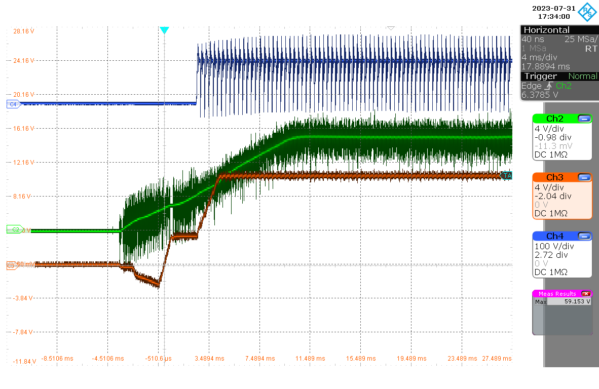
We do the dynamic load from 0A to 120A, step load 2A/us, 3kHz frequency 90% on /10% off, during the AC On/Off with dynamic load. We find the loading start from the VDD low than 3V, than the Vgs is going unstable. It has a negative gate voltage charge and discharge frequency. When we start the loading from the VDD high than 3V, then the gate voltage can work normal.

May I learn from you about what the reason cause the gate voltage become negative and charge/discharge frequency? I had tried to increase the BYP cap to 0.01uF, and VDD cap to 2.2uF, but all are not have any improve.


C4(Blue): Output current, C2(Green): VDD_TPS2412, C3(Orange): Vgs_OringFET

The loading start from the VDD low than 3V.

C4(Blue): Output current, C2(Green): VDD_TPS2412, C3(Orange): Vgs_OringFET

The loading start from the VDD low than 3V.

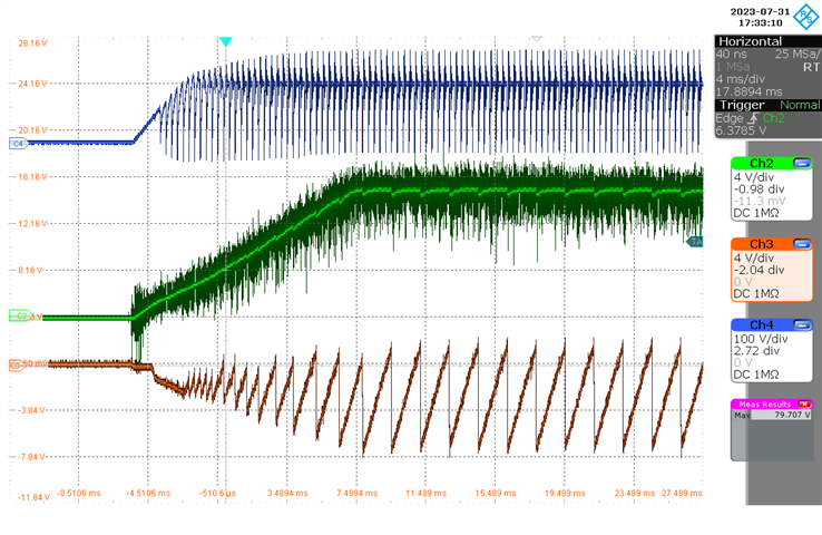
The loading start from the VDD high than 3V.

  • Hi Gary,

    Thanks for reaching out. Let me go through the issue description and get back to you by tomorrow.

  • Hi Gary,

    Can you please share the schematics of the circuit. 

    There is lot of oscillations/noise on the VDD which could be the reason for this behavior. Can you try adding a decoupling capacitor across VDD to GND to suppress the noise and check the behavior. 

  • Hi Praveen,

    I had sent the schematic in your email.

    As you mention that There is lot of oscillations/noise on the VDD. May I know why it can work normal when we start the loading from the VDD high than 3V? Could you explain more detail what is IC behavior let the Vgs going to negative voltage and frequently charge/discharge?

    BR, Thanks

  • Hi Gary,

    We can see in both the waveforms that the gate initially goes negative which is not expected. This could be because there is a lot of noise on the VDD pin which is also negative in the below highlighted region. 

    Is this actual noise on the VDD rail or noise coupled while measuring the signal ? The device is not rated for negative voltage on the VDD pin. So, the device can mis-behave or can get damaged when subjected to negative voltage on the VDD pin. 

    Also, the VDD pin provides power to the internal rails of the IC. When the VDD pin is noisy, the internal LDO's / voltage rails can become unstable and can will effect device operation. 

    How noisy is the input power rail ? If it is very noisy, probably the output capacitance of the upstream DC-DC converter is not high enough. Customer will have to increase the capacitance. 

    What is the resistance (R153) value between device GND and IC GND ? Can you make it 0 ohms and verify the IC behavior ?

  • Hi Praveen,

    I need to check again the VDD noisy. 

    The R153 is Open (No use). I will try to use 0 ohms and verify it. 

    BR, Gary

  • yes, please share the test results with R153 = 0 ohms and regarding the noise on the VDD pin.