


Electric vehicle (EV) charging systems are of two types: AC and DC. The AC charging system has to interface with the EV's internal on-board charger (OBC) before reaching the battery. The DC charging system interfaces with an external Electric Vehicle Supply Equipment (EVSE) with an AC/DC converter before bypassing the OBC and going directly to the battery.
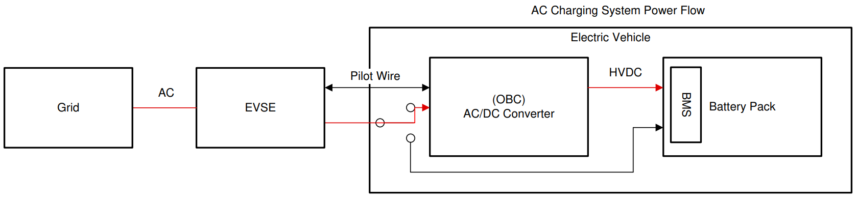
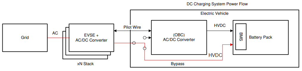
Figure 1. Electric Vehicle Supply Equipment (EVSE), On-Board Charger (OBC), Battery Management System (BMS)
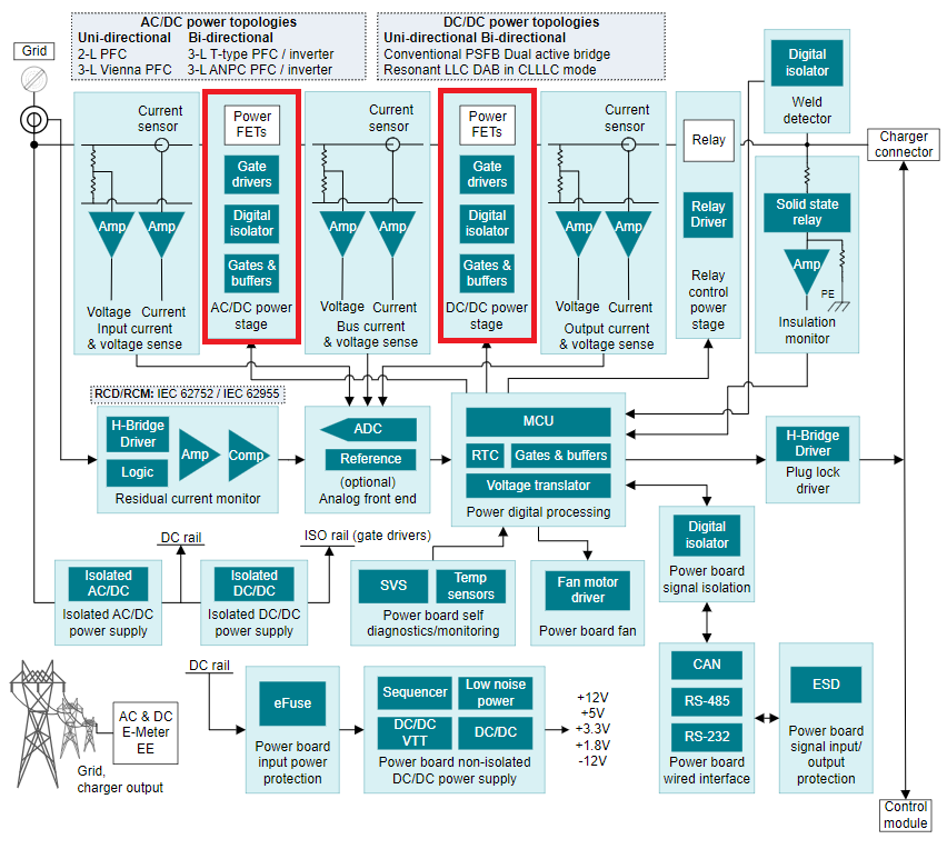
Figure 2. DC Fast Charging System Overall Block Diagram
Both systems require AC/DC Power Factor Correction (PFC) converter stage and DC/DC converter stage; in. This guide will focus on a DC EV charging system with an AC/DC PFC stage and DC/DC stage in the external EVSE. (For information on on-board chargers see TI.com’s page on OBC.) The FETs in a PFC work to alter the input voltage and currents phase to create a more ideal and harmonic AC signal which is then rectified into a DC signal potentially also using FETs. A DC/DC converter will use FETs to create a close to ideal and harmonic AC signal which will then be rectified. A gate driver should be used to drive the FETs in order to improve efficiency, reliability, and allow for further control. High drive strength will increase the speed at which the FET can switch and reduce switching losses. Negative voltage handling will allow for a more robust and noise immune system. A low delay matching time between output channels allows for each driver to efficiently control multiple drivers while reducing cost. Under-voltage lockout reduces conduction loss. The table below shows useful features of gate drivers and how they impact the overall design.
| Feature | Impact |
| Negative voltage handling | Robust and noise immune charger |
| Increased drive strength | Reduce rise and fall times, decrease switching loss |
| Delay matching | Minimize dead time, increase efficiency |
| Under Voltage Lockout (UVLO) | Limit conduction loss |
AC/DC PFC Converter Stage
Single Phase Totem Pole
The totem pole PFC uses the general layout of a full wave rectifier used in the conventional boost PFC, modified so two of the diodes are replaced by active GaN switches (S1 and S2) in a half-bridge configuration. The other two diodes are replaced by silicon FETs (S3 and S4) in a half-bridge configuration. S1 and S2 are driven in compliment and are used for the majority of correction; S3 and S4 are used for slowing and rectifying the signal. The benefit of this layout is increased efficiency and bidirectional operation. To review PFC circuit basics, see Power Factor Correction (PFC) Circuit Basics.
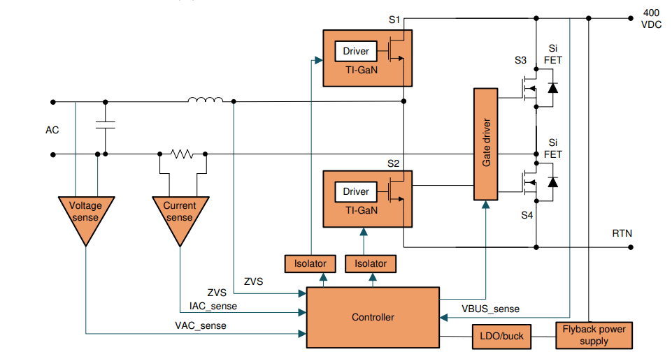
Figure 3. Single Phase Totem Pole Topology
GaN switches have zero-recovery reverse conduction allowing for running the topology in continuous-conduction mode (CCM). CCM is desirable as it has less power loss and higher filtering ability. See TI’s GaN switches with built in drivers. SiC switches also have zero-recovery reverse conduction and can be used instead of GaN in this topology.
Recommended Half-bridge Drivers
|
Device Name |
Recommended Supply Voltage |
Absolute Maximum Bus Voltage |
Drive Strength |
Propagation Delay |
|
10V-20V |
700V |
2.8A/1.8A |
100ns |
|
|
10V-17V |
640V |
4A |
90ns |
For more detail, see this bidirectional interleaved totem pole bridgeless PFC TIDM-1007.
DC/DC Converter Stage
Phase-Shifted Full Bridge (PSFB)
The PSFB is a part of the family of Dual Active Bridge (DAB) converters. In a PSFB, power is converted between different DC voltages at high efficiency by using switches on the "primary" side in phase. "Primary" refers to the input side, in this case at higher voltage. "Secondary" refers to the output side and in this case, the lower voltage. Primary and secondary sides are separated by a transformer.
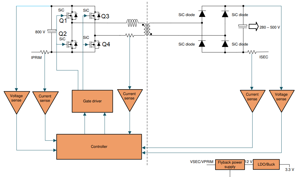
Figure 4. Phase-Shifted Full Bridge Topology
In figure 4 take note of primary-side FETs Q1-4. The controller will adjust the phase between the left and right pairs to modify the energy transfer at the transformer. Figure 5 shows the timing of the FETs. The diode structure on the secondary is rectification to provide a uniform DC signal.
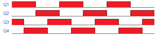
Figure 5. PSFB Timing Diagram
TI has multiple designs showing how to use PSFB topology with different gate drivers:
- TIDM-PSFB 400-V to 12-V DC/DC using low-side gate drivers.
- TIDM-BIDIR-400-12 bidirectional 400-V to 12-V DC/DC using low-side gate drivers.
- TIDM-01407 48-V to 12-V car battery converter with 120-V boot limit using half-bridge and low-side drivers.
Recommended Low-side Drivers
|
Device Name |
Recommended Supply Voltage |
Drive Strength |
Propagation Delay |
Use |
|
4.5V-26V |
5A |
17ns |
Dual channel |
|
|
4.5V-26V |
10A |
17ns |
Single channel |
Recommended Half-bridge Drivers
|
Device Name |
Recommended Supply Voltage |
Absolute Maximum Bus Voltage |
Drive Strength |
Propagation Delay |
Use |
|
10V-20V |
700V |
2.8A/1.8A |
100ns |
High voltage |
|
|
10V-17V |
640V |
4A |
90ns |
High voltage and high drive strength |
|
|
5.5V-16V |
120V |
3A |
16ns |
Low delay |
LLC Resonant Converter Stage
LLC Resonant Converters are part of the DAB family and are similar to PSFB. The main difference in the topology is the introduction of an LLC circuit at the primary-side transformer terminal. LLC Resonant Converters also have a more complex control system involving using different ranges of frequency for different results. Frequencies below the resonant frequency are used for soft switching on the secondary side at the cost of higher conduction loss. Frequencies above the resonant frequency are used for decreasing conduction loss at the cost of increased switching losses and hard switching. Frequencies near the resonant frequency are used for peak efficiency. LLC Resonant Converters are unidirectional due to the changes in topology and the control complexity.
Figure 6. LLC Resonant Converter
Recommended Low-side Drivers
|
Device Name |
Recommended Supply Voltage |
Drive Strength |
Propagation Delay |
Use |
|
4.5V-26V |
5A |
17ns |
Dual channel |
|
|
4.5V-26V |
10A |
17ns |
Single channel |
See the TIDM-1001 reference design 400-V to 12-V DC/DC converter using low-side gate drivers in an LLC topology.
This brief overview focuses on topologies that utilize a low-side or half-bridge gate driver. Other topologies make use of isolated gate drivers. To find out more about these topologies, see Power Topology Considerations for Electric Vehicle Charging Stations. For more resources on the topic of EV Charging Stations, see the DC fast charging power module overview.