


Dear experts,
Customers are now applying SN6505 in their automotive system, However, when testing the waveform on D1/D2 pins, waveform distortions were found;And their primary current is about 260 mA, The load current is less than 100 mA, 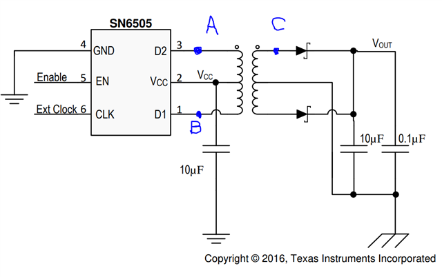
figure1 test circuit
The voltage waveform at point A or B to ground is similar, as shown in Figure 2:
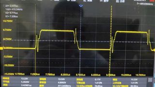
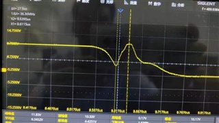
figure2 Voltage wave A(B) to GND
The voltage waveform C to ground shown in Figure 3:
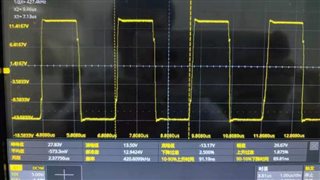
figure 3 Voltage wave C to GND (Transformer secondary side waveforms)
from figure2 and figure3, It seems that the voltage distortion on the primary side still affects the secondary side, Here are some preliminary assumptions:
1:Is the internal current limit triggered? What is the control logic inside the chip after triggering the current limit?
2: in this case (+) [FAQ] SN6505B-Q1: Driving waveform distortion at high ambient temperature - Isolation forum - Isolation - TI E2E support forums ,The speculation from the R&D is due to the diode reverse recovery current. My customer seems to be experiencing something similar to this case, especially in the low frequency oscillation section, but my customer is not experiencing high frequency noise issues. I was wondering if that was the same. Do you think the oscillation is caused by the diode reverse leakage current and leakage inductance ?(by the way, my customer unwilling to try other diode, and the diode ther use now has reverse current of 500uA, and the forward current can be 1A, the load current only 100mA, I don't think the diode selection is appropriate)
3:if oscillation was caused by diode reverse leakage current and leakage inductance, could you please give me information about the oscillation circuit and its timing?
4: The waveforms improved with the removal of the common-mode inductance shown in Figure 4, Can I think that the introduction of common-mode inductance increases the inductance of the oscillating loop, which is equivalent to increasing the leakage inductance of the transformer?As shown in Figure5
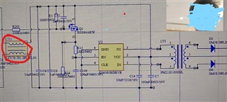
figure 4 common mode inductor position
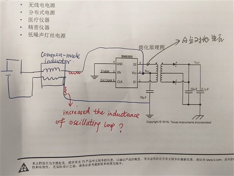
figure 5 common mode increase the inductance of oscillating loop(guess)
5:when customers change the transformers, the voltage wave A to GND have been improved(compare figure 6 ), but there are still some small spikes, not ideal, could you give some suggestions to further improve.
6:whether the waveform comparison of figure 2 and 6 can show that the shock is related to leakage?
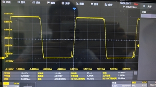
figure 6 waveform A to GND after change the transformer
Besides, my customers want some guidance about reduce the EMI when use the SN6505, can you provide relevant materials and test reports ,my email is :rickey-li@ti.com
Look forward to your reply soon, thank you in advance!
