This thread has been locked.

If you have a related question, please click the "Ask a related question" button in the top right corner. The newly created question will be automatically linked to this question.

TPS62872-Q1: TPS62872QWRXSRQ1 : WeBench simulation & Pspice Model

Part Number: TPS62872-Q1

Good morning,

I contact you because i can't simulate my TPS62872QWRXSRQ1 application.

In fact, the webench doesn't simulate this part and that is a problem for me. In the Design tools & simulation, there is the AVG simulation on Pspice and the transient on Simplis.

However, my company can't afford the license of Simplis and the simulation is too complex for the demo version. 

So, today, i can only simulate bode diagram. Is it because this component is too recent ? 

Is it possible to have the Pspice model of the TPS62872-Q1 transient analysis? 

Or is there any other way to simulate the transient ? 

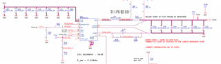
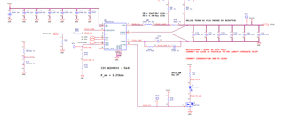
Please find below my design :

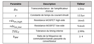
Here are my parameters : 

VIN = 5V

VOUT = 0.85V

IOUT = 6A

F_sw = 2.25MHz

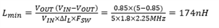
Below are the values calculated : 

Self : L = 330nH

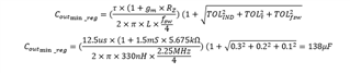
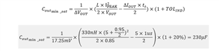
Output capacitor : Cout = 300uF

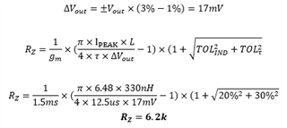
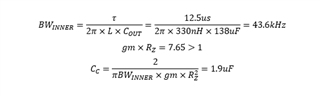
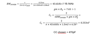
Compensation network : Rz = 5.1kOhm // CC = 2.2uF

Input capacitor : Cin = 122uF (for energy storage)

Thanks for your support,

Best regards,

NEANNE Florent

  • Hi,

    Thanks for reaching out to us.

    Yes, device is released recently and Webench model plan to release within 2 months.

    I have few feedback on your schematic. 

    • Compensation capacitance is 2.2uF. It should be 2.2nF .
    •  Reduce the inductor value as max inductance is 330nH. I would sugget to go for 220nH that can give tolerance window.

    Let me know if you looking for specific performance I can help you run simulation in SIMPLIS. 

    Best regards, 

    Tanvee

  • Hi,

    Thank you for your feedback.

    Please find below the detail of my calculations.

    Iout max = 6A

    • Compensation capacitance is 2.2uF. It should be 2.2nF .

    Do you agree on the resistor Rz value : 6.2k ? Here is my calculation : 

    Here is the output capacitor calculated according to the datasheet formula :

    If i follow the calculation of the compensation capacitance formula indicated on the datasheet : 

    As you see, Cc is closed to 2.2uF. Can you provide assistance on the calculation of compensation network values for Resistor and capacitor please ?

    •  Reduce the inductor value as max inductance is 330nH. I would sugget to go for 220nH that can give tolerance window.

    I found the minimum self inductor should be:

    As I didn't reach the 6A max, I prefered to choose a larger self value to not be in discontinuous mode. What is the impact of reducing the self value tolerance window ?

    Thank you in advance for your help.

    Best regards,

    Florent NEANNE

  • Hi Florent,

    For Output Cout calculation have to done for both equation 13 and 15. Max value should be selected from both equation and according to you operating condition it seems you will max around 362uF (output caps).

    Cc equation is correct but I think unit is not selected correctly gm is 1.5ms; BW in kHz and Rz in KHz(in square) will give value in ~nF. Can you check units used for calculation.

    Thanks,

    Tanvee

  • Hi Tanvee,

    Thank you for your return.

    I added calculation with equation 15 : 

    I choose to select Cout around 300uF.

    Regarding Cc indeed I finally found : 470pF : 

    Finally, please find below my schematic : 

    Can you provide simulation with simplis please : 

    - Startup 

    - Load transient

    - Steady state

    - Line trans

    - Bode diagram 

    I would like to know if the system is stable regarding the calculation of the compensation network components

    Thanks in advance,

    Best regards

  • Hi ,

    Can you share load profile (load step , slew rate ) for transient simulation?

    Thanks,

    Tanvee

  • Hi Tanvee, 

    I use an Ultrascale + FPGA and I expect the full power core load step can rise up to 5A/us.

    Regards,

    Florent

  • Hi Florent,

    I will sugget to reduce the inductor value to 220nH. 330nH with +/-20% tolerance is outside datasheet recommendation.

    I will run simulation for all condition and send you result today.

    Thanks,

    Tanvee 

  • Hi Florent,

    Please find the simulation result for operating condition.

    /TPS62872_Q1_Simulation-result.pptx

    Best regards,

    Tanvee

  • Hi Tanvee,

    Thank you verry much for your feedback.

    Can you help me to understand the gain margin on your last simulation ?

    I can identify the phase margin but I have difficulties to interprate the gain margin ?

    Can you provide also a simulation file with a 330uH inductance value in order to have a comparison please?

    Thanks  for your support,

    Best regards

    Florent 

  • Hi Florent,

    GM will not impact much on device stability. It is around 10dB.

    I have attached the  simulation profile in presentation that can work in SIMPLIS demo revision.

    Can you run simulation on it ? and we also have TI PSPICE model which is can help you to run transient simulation.

    MAX values will affect device in the for corner case and reliability. can you share purpose for higher inductor value? 

    Thanks,

    Tanvee

  • Hi Tanvee,

    Thank you for your feedback.

    Higher inductor values can be required if a lower current is used.

    It is hard for now to determine the correct current consumption on our design because we are in the development phase with our Xilinx UltraScale+.

    The DC-DC converter is used to supply the core voltage of the FPGA.

    Thanks,

    Florent

  • Hi Florent,

    Understood. Let me know if you need further help on my end.

    Thanks,

    Tanvee