Hello all,
I've been diagnosing a befuddling issue with a BQ76942. We're becoming familiar with and configuring these chips on a small run of prototype boards. I've successfully ready cell voltages, temp values, pack current, etc.
We're controlling the chip with an STM32G474 via I2C. I used the STM32 example code as a starting point which has been a huge help.
First, let me describe the issue when I'm using the standard BQInit code provided in the example except I changed the VCellMode register to reflect the number of cells in my pack (4s) so the chip doesn't throw UV errors.
The code executes like this: first the BQ_Reset pin is released and then the TS2 pin is toggled low then high impedance. I don't see anything in the datasheet that shows I should have to toggle this but it seems to be the only thing that wakes the chip. Then the BQReset and BQInit functions are executed. After executing the init I disable sleep mode then the code enters the main loop.
In the main loop I read some status and error registers and toggle the command DSGTEST and CHGTEST off and on every second. The DSG and CHG variables are toggling correctly as read by the ReadFETStatus function and the 0x0057 Manufacturing Status register. The FET EN bit is deasserted in that register as well which I believe means the device is in test mode. Measuring the board, the DSG FET is not closing completely. It's gate voltage does not rise above 14 volts (pack voltage is ~14.7). The charge pump as measure at CP1 toggles between 25.5 and ~14 volts. It seems that the charge pump is shutting off when the FETs are enabled.
Here is the code:
void bmsInit()
{
	/* Initiate and set up the BMS hardware
	 * Load config data from EEPROM
	 * Read DIP switches and configure hardware
	 */

	if(__HAL_PWR_GET_FLAG(PWR_FLAG_SB) != RESET)
	{
		test = 1;
	}
	HAL_Delay(1);
	HAL_TIM_Base_Start_IT(&htim4);
	BQ769x2_ReleaseShutdownPin();//Release the BQ_Reset Pin
	delayUS(60000);
	HAL_GPIO_WritePin(GPIO2_GPIO_Port, GPIO2_Pin,GPIO_PIN_RESET);//Toggle the TS2 Pin Low
	delayUS(60000);
	HAL_GPIO_WritePin(GPIO2_GPIO_Port, GPIO2_Pin,GPIO_PIN_SET);//Toggle TS2 to high impedance
	// Initialize battery controller chip
	CommandSubcommands(BQ769x2_RESET);  // Resets the BQ769x2 registers
	delayUS(60000);
	BQ769x2_Init();  // Configure all of the BQ769x2 register settings
	delayUS(10000);
	CommandSubcommands(SLEEP_DISABLE); // Sleep mode is enabled by default. For this example, Sleep is disabled to demonstrate full-speed measurements in Normal mode.
	delayUS(60000); delayUS(60000); delayUS(60000); delayUS(60000);  //wait to start measurements after FETs close
void BQ769x2_Init() {
	// Configures all parameters in device RAM

	// Enter CONFIGUPDATE mode (Subcommand 0x0090) - It is required to be in CONFIG_UPDATE mode to program the device RAM settings
	// See TRM for full description of CONFIG_UPDATE mode
	CommandSubcommands(SET_CFGUPDATE);

	// After entering CONFIG_UPDATE mode, RAM registers can be programmed. When programming RAM, checksum and length must also be
	// programmed for the change to take effect. All of the RAM registers are described in detail in the BQ769x2 TRM.
	// An easier way to find the descriptions is in the BQStudio Data Memory screen. When you move the mouse over the register name,
	// a full description of the register and the bits will pop up on the screen.

	// 'Power Config' - 0x9234 = 0x2D80
	// Setting the DSLP_LDO bit allows the LDOs to remain active when the device goes into Deep Sleep mode
  	// Set wake speed bits to 00 for best performance
	BQ769x2_SetRegister(PowerConfig, 0x2D80, 2);

	// 'REG0 Config' - set REG0_EN bit to enable pre-regulator
	BQ769x2_SetRegister(REG0Config, 0x01, 1);

	// 'REG12 Config' - Enable REG1 with 3.3V output (0x0D for 3.3V, 0x0F for 5V)
	BQ769x2_SetRegister(REG12Config, 0x0D, 1);

	// Set DFETOFF pin to control BOTH CHG and DSG FET - 0x92FB = 0x42 (set to 0x00 to disable)
	BQ769x2_SetRegister(DFETOFFPinConfig, 0x42, 1);

	// Set up ALERT Pin - 0x92FC = 0x2A
	// This configures the ALERT pin to drive high (REG1 voltage) when enabled.
	// The ALERT pin can be used as an interrupt to the MCU when a protection has triggered or new measurements are available
	BQ769x2_SetRegister(ALERTPinConfig, 0x2A, 1);

	// Set TS1 to measure Cell Temperature - 0x92FD = 0x07
	BQ769x2_SetRegister(TS1Config, 0x07, 1);

	// Set TS3 to measure FET Temperature - 0x92FF = 0x0F
	BQ769x2_SetRegister(TS3Config, 0x0F, 1);

	// Set HDQ to measure Cell Temperature - 0x9300 = 0x07
	BQ769x2_SetRegister(HDQPinConfig, 0x00, 1);  // No thermistor installed on EVM HDQ pin, so set to 0x00

	// 'VCell Mode' - Enable 16 cells - 0x9304 = 0x0000; Writing 0x0000 sets the default of 16 cells
	BQ769x2_SetRegister(VCellMode, 0x0207, 2);

	// Enable protections in 'Enabled Protections A' 0x9261 = 0xBC
	// Enables SCD (short-circuit), OCD1 (over-current in discharge), OCC (over-current in charge),
	// COV (over-voltage), CUV (under-voltage)
	BQ769x2_SetRegister(EnabledProtectionsA, 0xBC, 1); //DISABLED, MUST BE REENABLED, OR ELSE

	// Enable all protections in 'Enabled Protections B' 0x9262 = 0xF7
	// Enables OTF (over-temperature FET), OTINT (internal over-temperature), OTD (over-temperature in discharge),
	// OTC (over-temperature in charge), UTINT (internal under-temperature), UTD (under-temperature in discharge), UTC (under-temperature in charge)
	BQ769x2_SetRegister(EnabledProtectionsB, 0xF7, 1);

	// 'Default Alarm Mask' - 0x..82 Enables the FullScan and ADScan bits, default value = 0xF800
	BQ769x2_SetRegister(DefaultAlarmMask, 0xF882, 2);

	// Set up Cell Balancing Configuration - 0x9335 = 0x03   -  Automated balancing while in Relax or Charge modes
	// Also see "Cell Balancing with BQ769x2 Battery Monitors" document on ti.com
	BQ769x2_SetRegister(BalancingConfiguration, 0x03, 1);

	// Set up CUV (under-voltage) Threshold - 0x9275 = 0x31 (2479 mV)
	// CUV Threshold is this value multiplied by 50.6mV
	BQ769x2_SetRegister(CUVThreshold, 0x31, 1);

	// Set up COV (over-voltage) Threshold - 0x9278 = 0x55 (4301 mV)
	// COV Threshold is this value multiplied by 50.6mV
	BQ769x2_SetRegister(COVThreshold, 0x55, 1);

	// Set up OCC (over-current in charge) Threshold - 0x9280 = 0x05 (10 mV = 10A across 1mOhm sense resistor) Units in 2mV
	BQ769x2_SetRegister(OCCThreshold, 0x05, 1);

	// Set up OCD1 Threshold - 0x9282 = 0x0A (20 mV = 20A across 1mOhm sense resistor) units of 2mV
	BQ769x2_SetRegister(OCD1Threshold, 0x0A, 1);

	// Set up SCD Threshold - 0x9286 = 0x05 (100 mV = 100A across 1mOhm sense resistor)  0x05=100mV
	BQ769x2_SetRegister(SCDThreshold, 0x05, 1);

	// Set up SCD Delay - 0x9287 = 0x03 (30 us) Enabled with a delay of (value - 1) * 15 µs; min value of 1
	BQ769x2_SetRegister(SCDDelay, 0x03, 1);

	// Set up SCDL Latch Limit to 1 to set SCD recovery only with load removal 0x9295 = 0x01
	// If this is not set, then SCD will recover based on time (SCD Recovery Time parameter).
	BQ769x2_SetRegister(SCDLLatchLimit, 0x01, 1);

	// Exit CONFIGUPDATE mode  - Subcommand 0x0092
	CommandSubcommands(EXIT_CFGUPDATE);
}
while (1)
  {
    /* USER CODE END WHILE */

    /* USER CODE BEGIN 3 */
	time = HAL_GetTick();

	BQ769x2_ReadPFStatus();
	BQ769x2_ReadFETStatus();
	wake_status = BQ769x2_ReadWakeStatus();

	if(time-last_switch_time>1000){
		CommandSubcommands(DSGTEST);
		CommandSubcommands(CHGTEST);
		last_switch_time = time;
	}

	BQ769x2_ReadManufacturingStatus();

	AlarmBits = BQ769x2_ReadAlarmStatus();
	if (AlarmBits & 0x80) {  // Check if FULLSCAN is complete. If set, new measurements are available
		BQ769x2_ReadAllVoltages();
		Pack_Current = BQ769x2_ReadCurrent();
		Temperature[0] = BQ769x2_ReadTemperature(TS1Temperature);
		Temperature[1] = BQ769x2_ReadTemperature(IntTemperature);
		DirectCommands(AlarmStatus, 0x0080, W_BQ);  // Clear the FULLSCAN bit
	}

	if (AlarmBits & 0xC000) {  // If Safety Status bits are showing in AlarmStatus register
		BQ769x2_ReadSafetyStatus(); // Read the Safety Status registers to find which protections have triggered
		if (ProtectionsTriggered & 1) {
			DirectCommands(AlarmStatus, 0xF800, W_BQ); // Clear the Safety Status Alarm bits.
		}
	}
I've also created my own configuration of the BQ Init function. Here it is below. Essentially I was trying to configure the chip to run in normal mode using MfgStatusInit and then use the ALL_FETS_ON command to turn on the FETs. However, as soon as the Init function reaches EXIT_CFGUPDATE the charge pumps shuts off.
void BQ769x2_Init() {
	// Configures all parameters in device RAM

	// Enter CONFIGUPDATE mode (Subcommand 0x0090) - It is required to be in CONFIG_UPDATE mode to program the device RAM settings
	// See TRM for full description of CONFIG_UPDATE mode
	CommandSubcommands(SET_CFGUPDATE);

	// After entering CONFIG_UPDATE mode, RAM registers can be programmed. When programming RAM, checksum and length must also be
	// programmed for the change to take effect. All of the RAM registers are described in detail in the BQ769x2 TRM.
	// An easier way to find the descriptions is in the BQStudio Data Memory screen. When you move the mouse over the register name,
	// a full description of the register and the bits will pop up on the screen.

	// 'Power Config' - 0x9234 = 0x2D80
	// Setting the DSLP_LDO bit allows the LDOs to remain active when the device goes into Deep Sleep mode
  	// Set wake speed bits to 00 for best performance
	BQ769x2_SetRegister(PowerConfig, 0x2C80, 2);

	// 'REG0 Config' - set REG0_EN bit to enable pre-regulator
	BQ769x2_SetRegister(REG0Config, 0x01, 1);

	// 'REG12 Config' - Enable REG1 with 3.3V output (0x0D for 3.3V, 0x0F for 5V)
	BQ769x2_SetRegister(REG12Config, 0x0D, 1);

	// Set DFETOFF pin to control BOTH CHG and DSG FET - 0x92FB = 0x42 (set to 0x00 to disable)
	BQ769x2_SetRegister(DFETOFFPinConfig, 0x00, 1);

	// Set up ALERT Pin - 0x92FC = 0x2A
	// This configures the ALERT pin to drive high (REG1 voltage) when enabled.
	// The ALERT pin can be used as an interrupt to the MCU when a protection has triggered or new measurements are available
	BQ769x2_SetRegister(ALERTPinConfig, 0x2A, 1);

	// Set TS1 to measure Cell Temperature - 0x92FD = 0x07
	BQ769x2_SetRegister(TS1Config, 0x07, 1);

	// Set TS3 to measure FET Temperature - 0x92FF = 0x0F
	BQ769x2_SetRegister(TS3Config, 0x00, 1);

	// Set HDQ to measure Cell Temperature - 0x9300 = 0x07
	BQ769x2_SetRegister(HDQPinConfig, 0x00, 1);  // No thermistor installed on EVM HDQ pin, so set to 0x00

	// 'VCell Mode' - Enable 16 cells - 0x9304 = 0x0000; Writing 0x0000 sets the default of 16 cells
	BQ769x2_SetRegister(VCellMode, 0x0207, 2);//

	// Enable protections in 'Enabled Protections A' 0x9261 = 0xBC
	// Enables SCD (short-circuit), OCD1 (over-current in discharge), OCC (over-current in charge),
	// COV (over-voltage), CUV (under-voltage)
	BQ769x2_SetRegister(EnabledProtectionsA, 0xBC, 1);

	// Enable all protections in 'Enabled Protections B' 0x9262 = 0xF7
	// Enables OTF (over-temperature FET), OTINT (internal over-temperature), OTD (over-temperature in discharge),
	// OTC (over-temperature in charge), UTINT (internal under-temperature), UTD (under-temperature in discharge), UTC (under-temperature in charge)
	BQ769x2_SetRegister(EnabledProtectionsB, 0xF7, 1);

	// 'Default Alarm Mask' - 0x..82 Enables the FullScan and ADScan bits, default value = 0xF800
	BQ769x2_SetRegister(DefaultAlarmMask, 0xF882, 2);

	// Set up Cell Balancing Configuration - 0x9335 = 0x03   -  Automated balancing while in Relax or Charge modes
	// Also see "Cell Balancing with BQ769x2 Battery Monitors" document on ti.com
	BQ769x2_SetRegister(BalancingConfiguration, 0x03, 1);

	// Set up CUV (under-voltage) Threshold - 0x9275 = 0x31 (2479 mV)
	// CUV Threshold is this value multiplied by 50.6mV
	BQ769x2_SetRegister(CUVThreshold, 0x31, 1);

	// Set up COV (over-voltage) Threshold - 0x9278 = 0x55 (4301 mV)
	// COV Threshold is this value multiplied by 50.6mV
	BQ769x2_SetRegister(COVThreshold, 0x55, 1);

	// Set up OCC (over-current in charge) Threshold - 0x9280 = 0x05 (10 mV = 10A across 1mOhm sense resistor) Units in 2mV
	BQ769x2_SetRegister(OCCThreshold, 0x05, 1);

	// Set up OCD1 Threshold - 0x9282 = 0x0A (20 mV = 20A across 1mOhm sense resistor) units of 2mV
	BQ769x2_SetRegister(OCD1Threshold, 0x0A, 1);

	// Set up SCD Threshold - 0x9286 = 0x05 (100 mV = 100A across 1mOhm sense resistor)  0x05=100mV
	BQ769x2_SetRegister(SCDThreshold, 0x05, 1);

	// Set up SCD Delay - 0x9287 = 0x03 (30 us) Enabled with a delay of (value - 1) * 15 µs; min value of 1
	BQ769x2_SetRegister(SCDDelay, 0x1e, 1);

	// Set up SCDL Latch Limit to 1 to set SCD recovery only with load removal 0x9295 = 0x01
	// If this is not set, then SCD will recover based on time (SCD Recovery Time parameter).
	BQ769x2_SetRegister(SCDLLatchLimit, 0xFF, 1); //Needs to be decreased

	//Change the CC gain to match the sense resistor on the board for current measurement
	//CCGain value is .37842
	BQ769x2_SetRegister(CCGain, 0x40f23055, 4);

	//Change the Capacity Gain for correct coulomb counting, it is based on CC Gain
	//Current Gain value is 112868.1614
	BQ769x2_SetRegister(CapacityGain, 0x4a09c74d, 4);

	//Disable Sleep
	CommandSubcommands(SLEEP_DISABLE);

	///////////////////////////////////////////////////////////////////////////////////
	//SET UP THE FETS

	//Set the Fet Options Register
	//00001101
	BQ769x2_SetRegister(FETOptions, 0x0d, 1);

	//CommandSubcommands(FET_ENABLE);
	BQ769x2_SetRegister(MfgStatusInit,0x0050,2);

	//Turn on the charge pump
	//00000111
	BQ769x2_SetRegister(ChgPumpControl, 0x07, 1);
	HAL_Delay(2000);


	// Exit CONFIGUPDATE mode  - Subcommand 0x0092


	CommandSubcommands(EXIT_CFGUPDATE);

}
I've been up and down the TRM a hundred times and am at a loss, so your help is appreciated.
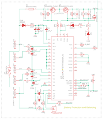
Included below is our schematic.