This thread has been locked.
If you have a related question, please click the "Ask a related question" button in the top right corner. The newly created question will be automatically linked to this question.
Hi TPS6594 Champ
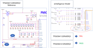
A customer is developing a Custom Board using TDA4AL and TPS65941120RWERQ1.
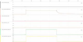
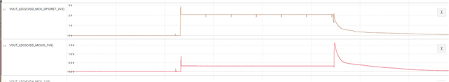
PMIC Default Power is not output, so I'm checking it, what other signals should I check besides nPowerON/ENABLE?
Can it be shipped without a Default Setting value on the PMIC?
Would it be possible if I set it to i2c additionally because there is no Default Power Setting value? Please let me know the information such as that.
Thanks.
Regards,
Jack
LP876411B4RQKRQ1 also does not work. The Step-Down Power Switching is not functional.
How can I check if it's OTP programmed?
Regards,
Jack
For all 3 devices, do their internal LDOs come up?
For the TPS6594xxxx devices, VOUT_LDOVINT and VOUT_LDORTC are on pins 2 and 3. They should both be 1.8V.
For the LP8764xxxx device, VOUT_LDO is on pin 20. It should also be 1.8V.
After confirming the above voltage measurements, please follow use these 2 FAQ posts for guidance on connecting to the PMIC I2C lines to read the interrupt registers.
Hi Michael
Thanks for your kind answer.
Customer will get back to us with these LDO output check.
By the way, a customer purchased TPS6594, LP8764 PMIC from an Open Market such as digikey mouser, and they asked if these parts are programmed and shipped with default setting in OTP in the NVM.
Can I check the NVM default setting through the attached picture?
Do you ship the blank pmic so that customers can program themselves with OTP?
Please answer.
Thanks.
Regards,
Jack
Hi Michael
Please find their measurement.
- PMIC SIDE-A : VOUT_LDOVINT --> 1.8V , VOUT_LDORTC --> 2.0V
- PMIC SIDE-B : VOUT_LDOVINT --> 1.8V , VOUT_LDORTC --> 2.0V
- LP8764xxxx device : VOUT_LDO --> 1.8V
Also let us know what should they check if VOUT_LDORTC is 2.0V.
Thanks.
Regards,
Jack
Hi Michael
Please find their schematic for PMIC side.
Can you please check if there's critical mistake from PMIC side?
Thanks.
Regards,
Jack
Can I check the NVM default setting through the attached picture?
Based on the pictures, the NVM settings should match those in this users guide: https://www.ti.com/lit/pdf/slvucj9
Do you ship the blank pmic so that customers can program themselves with OTP?
This is possible. The OPN for a "blank" PMIC is the TPS65940400.
Also let us know what should they check if VOUT_LDORTC is 2.0V.
Can the customer provide a scope shot of VSYS_3V3 and the VOUT_LDORTC on PMIC-A and PMIC-B? At 2.0V, I am concerned about noise or poor grounding of the device.
The LP8764 device not powering up makes sense since it is expecting SPMI communication from the other two PMICs.
Hi Michael,
We tested LP876411B4-Q1 replacement with TI sample, but it does not work properly.
1. Test after replacing LP876411B4-Q1 on an existing board --> Inoperable (VOUT_LDO alone is 1.8V output)
2. Test after configuring only LP876411B4-Q1 circuit on Bare PCB --> inoperable (VOUT_LDO alone is 1.8V output)
Each power source has been measured.
Q1) Is there a timing when FB_B3 and FB_B4 are powered or does this affect the operation?
(Wave Note, Same Timing as VSYS_3V3)
Q2) Are there any conditions that affect GPIO, I2C, nINT & other behavior?
Q3) LP876411B4-Q1 Please advise what is required for initial operation.
If you have any information you need for advice, please request it.
Additional Questions : TPS65941120RWERQ1
The OVPGDRV + VSYS_SENCE circuit seems to affect the operation.
On the previous model, TPS65941212RWERQ1, the circuit configuration as in the eintelligence Model allowed for operation.
However, it does not work with TPS65941120RWERQ1.
Q1) Does it work if apply R43 --> Open, D3 --> 0 ohm in the reference circuit?
The LP876411B5 requires both a working TPS65941120 and TPS65941421 to be present.
The LP876411B4 is expecting a TPS65941213 to be present.
None of the above listed PMICs will work on their own. Please note that the LP876411B4 and LP876411B5 are not interchangeable.
The OVPGDRV + VSYS_SENCE circuit seems to affect the operation.
Why do you think this is affecting the operation? If VCCA measures 3.3V, then the safety FET circuit is working.
I previously asked about a scope shots of the VOUT-LDO on PMIC-A and PMIC-B. This would be the TPS65941120 and TPS65941421. Can the customer provide these scope shots? Please use a time and voltage scale that would allow me to check for noise.
Can customer read the interrupt registers from the PMICs?
Hi Michael,
Sorry, I didn't check the old question history.
The customer is preparing to read the interrupt register.
I will prepare scope shots of PMIC-A and B.
- LP876411B4 is a typing error.
The customer has read the register with the I2C.
Please advise us on how to take further action.
Waveform are being checked.
1. TPS65941120-Q1 Ti337 W272 G4
- pmicRead :: device id:0x48, DEV_REV: 0x00, NVM_CODE_1:0x00, NVM_CODE_2:0x00
2. TPS65941421-Q1 TI357 W344 G4
- PmicRead :: device id:0x4c, DEV_REV: 0x00, NVM_CODE_1:0x00, NVM_CODE_2:0x00
3. LP876411B5-Q1 Ti 34J P7XN
- pmicRead :: device id:0x58, DEV_REV: 0x86, NVM_CODE_1:0xb5, NVM_CODE_2:0x02
Please check if the PMIC part number to be used for TDA4AL88 is correct.
(TPS65941120-Q1 + TPS65941421-Q1 + LP876411B5-Q1)
AP : TDA4AL88TGAALZQ1 32P0VSS 206
Reference : PROC118E3(001)_SCH
PMIC LDO OUT
TPS65941120RWERQ1
TPS65941421RWERQ1
LP876411B4RQKRQ1
Register value
* PMIC A: TPS65941120RWERQ1 User Registers ( i2c device id: 0x48 ) DEV_REV: 0x00, NVM_CODE_1:0x00, NVM_CODE_2:0x00 BUCK1_CTRL:0x00, BUCK1_CONF:0x00, BUCK2_CTRL:0x00, BUCK2_CONF:0x00, BUCK3_CTRL:0x00, BUCK3_CONF:0x00, BUCK4_CTRL:0x00, BUCK4_CONF:0x00, BUCK5_CTRL:0x00, BUCK5_CONF:0x00 BUCK1_VOUT_1:0x00, BUCK1_VOUT_2:0x00, BUCK2_VOUT_1:0x00, BUCK2_VOUT_2:0x00, BUCK3_VOUT_1:0x00, BUCK3_VOUT_2:0x00, BUCK4_VOUT_1:0x00, BUCK4_VOUT_2:0x00, BUCK5_VOUT_1:0x00, BUCK5_VOUT_2:0x00 BUCK1_PG_WINDOW:0x00, BUCK2_PG_WINDOW:0x00, BUCK3_PG_WINDOW:0x00, BUCK4_PG_WINDOW:0x00, BUCK5_PG_WINDOW:0x00 LDO1_CTRL:0x00, LDO2_CTRL:0x00, LDO3_CTRL:0x00, LDO4_CTRL:0x00 LDORTC_CTRL:0x00 LDO1_VOUT:0x00, LDO2_VOUT:0x00, LDO3_VOUT:0x00, LDO4_VOUT:0x00 LDO1_PG_WINDOW:0x00, LDO2_PG_WINDOW:0x00, LDO3_PG_WINDOW:0x00, LDO4_PG_WINDOW:0x00 VCCA_VMON_CTRL:0x00, VCCA_PG_WINDOW:0x00 GPIO1_CONF:0x00, GPIO2_CONF:0x00, GPIO3_CONF:0x00, GPIO4_CONF:0x00 GPIO5_CONF:0x00, GPIO6_CONF:0x00, GPIO7_CONF:0x00, GPIO8_CONF:0x00 GPIO9_CONF:0x00, GPIO10_CONF:0x00, GPIO11_CONF:0x00, NPWRON_CONF:0x00 GPIO_OUT_1:0x00, GPIO_OUT_2:0x00, GPIO_IN_1:0x00, GPIO_IN_2:0x00 STAT_BUCK1_2:0x00, STAT_BUCK3_4:0x00, STAT_BUCK5:0x00, STAT_LDO1_2:0x00, STAT_LDO3_4:0x00, STAT_VMON:0x00, STAT_STARTUP:0x00 STAT_MISC:0x00, STAT_MODERATE_ERR:0x00, STAT_SEVERE_ERR:0x00, STAT_READBACK_ERR:0x00 * PMIC B: TPS65941421RWERQ1 User Registers ( i2c device id: 0x4C ) DEV_REV: 0x00, NVM_CODE_1:0x00, NVM_CODE_2:0x00 BUCK1_CTRL:0x00, BUCK1_CONF:0x00, BUCK2_CTRL:0x00, BUCK2_CONF:0x00, BUCK3_CTRL:0x00, BUCK3_CONF:0x00, BUCK4_CTRL:0x00, BUCK4_CONF:0x00, BUCK5_CTRL:0x00, BUCK5_CONF:0x00 BUCK1_VOUT_1:0x00, BUCK1_VOUT_2:0x00, BUCK2_VOUT_1:0x00, BUCK2_VOUT_2:0x00, BUCK3_VOUT_1:0x00, BUCK3_VOUT_2:0x00, BUCK4_VOUT_1:0x00, BUCK4_VOUT_2:0x00, BUCK5_VOUT_1:0x00, BUCK5_VOUT_2:0x00 BUCK1_PG_WINDOW:0x00, BUCK2_PG_WINDOW:0x00, BUCK3_PG_WINDOW:0x00, BUCK4_PG_WINDOW:0x00, BUCK5_PG_WINDOW:0x00 LDO1_CTRL:0x00, LDO2_CTRL:0x00, LDO3_CTRL:0x00, LDO4_CTRL:0x00 LDORTC_CTRL:0x00 LDO1_VOUT:0x00, LDO2_VOUT:0x00, LDO3_VOUT:0x00, LDO4_VOUT:0x00 LDO1_PG_WINDOW:0x00, LDO2_PG_WINDOW:0x00, LDO3_PG_WINDOW:0x00, LDO4_PG_WINDOW:0x00 VCCA_VMON_CTRL:0x00, VCCA_PG_WINDOW:0x00 VMON1_PG_WINDOW:0x00, VMON1_PG_LEVEL:0x00, VMON2_PG_WINDOW:0x00, VMON2_PG_LEVEL:0x00 GPIO1_CONF:0x00, GPIO2_CONF:0x00, GPIO3_CONF:0x00, GPIO4_CONF:0x00 GPIO5_CONF:0x00, GPIO6_CONF:0x00, GPIO7_CONF:0x00, GPIO8_CONF:0x00 GPIO9_CONF:0x00, GPIO10_CONF:0x00, GPIO11_CONF:0x00, NPWRON_CONF(ENABLE_CONF):0x00 GPIO_OUT_1:0x00, GPIO_OUT_2:0x00, GPIO_IN_1:0x00, GPIO_IN_2:0x00 STAT_BUCK1_2:0x00, STAT_BUCK3_4:0x00, STAT_BUCK5:0x00, STAT_LDO1_2:0x00, STAT_LDO3_4:0x00, STAT_VMON:0x00, STAT_STARTUP:0x00 STAT_MISC:0x00, STAT_MODERATE_ERR:0x00, STAT_SEVERE_ERR:0x00, STAT_READBACK_ERR:0x00 * PMIC C: LP876411B4RQKRQ1 User Registers ( i2c device id: 0x58 ) DEV_REV: 0x80, NVM_CODE_1:0x01, NVM_CODE_2:0x02 BUCK1_CTRL:0x22, BUCK1_CONF:0x3b, BUCK2_CTRL:0x02, BUCK2_CONF:0x13, BUCK3_CTRL:0x02, BUCK3_CONF:0x20, BUCK4_CTRL:0x00, BUCK4_CONF:0x02 BUCK1_VOUT_1:0x01, BUCK1_VOUT_2:0x20, BUCK2_VOUT_1:0x11, BUCK2_VOUT_2:0x23, BUCK3_VOUT_1:0x00, BUCK3_VOUT_2:0x00, BUCK4_VOUT_1:0x00, BUCK4_VOUT_2:0x00 BUCK1_PG_WINDOW:0x1b, BUCK2_PG_WINDOW:0x1b, BUCK3_PG_WINDOW:0x00, BUCK4_PG_WINDOW:0x00 VCCA_VMON_CTRL:0x00, VCCA_PG_WINDOW:0x35 VMON1_PG_WINDOW:0x00, VMON1_PG_LEVEL:0x00, VMON2_PG_WINDOW:0x00, VMON2_PG_LEVEL:0x00 GPIO1_CONF:0x00, GPIO2_CONF:0x18, GPIO3_CONF:0x18, GPIO4_CONF:0x18 GPIO5_CONF:0x18, GPIO6_CONF:0x18, GPIO7_CONF:0x18, GPIO8_CONF:0x20 GPIO9_CONF:0x20, GPIO10_CONF:0x18, ENABLE_CONF:0x00 GPIO_OUT_1:0x00, GPIO_OUT_2:0x00, GPIO_IN_1:0x00, GPIO_IN_2:0x00 STAT_BUCK1_2:0x00, STAT_BUCK3_4:0x00, STAT_VMON:0x00, STAT_STARTUP:0x00 STAT_MISC:0x00, STAT_MODERATE_ERR:0x00, STAT_SEVERE_ERR:0x00, STAT_READBACK_ERR:0x00 SoM I2C ADDRESS TABLE : pmic 이외의 read된 device id는 eeprom 등 다른 것입니다. - PMIC A: TPS65941120RWERQ1 ( 0x48, 0x49, 0x4A & 0x4B ) - PMIC B: TPS65941421RWERQ1 ( 0x4C, 0x4D, 0x4E & 0x4F ) - PMIC C: P876411A5RQKRQ1 ( 0x58, 0x59, 0x5A & 0x5B ) pmicRead :: device id:0x48, DEV_REV: 0x00, NVM_CODE_1:0x00, NVM_CODE_2:0x00 pmicRead :: device id:0x49, DEV_REV: 0x00, NVM_CODE_1:0x00, NVM_CODE_2:0x00 pmicRead :: device id:0x4a, DEV_REV: 0x00, NVM_CODE_1:0x00, NVM_CODE_2:0x00 pmicRead :: device id:0x4b, DEV_REV: 0x00, NVM_CODE_1:0x00, NVM_CODE_2:0x00 pmicRead :: device id:0x4c, DEV_REV: 0x00, NVM_CODE_1:0x00, NVM_CODE_2:0x00 pmicRead :: device id:0x4d, DEV_REV: 0x00, NVM_CODE_1:0x00, NVM_CODE_2:0x00 pmicRead :: device id:0x4e, DEV_REV: 0x00, NVM_CODE_1:0x00, NVM_CODE_2:0x00 pmicRead :: device id:0x4f, DEV_REV: 0x00, NVM_CODE_1:0x00, NVM_CODE_2:0x00 pmicRead :: device id:0x50, DEV_REV: 0xff, NVM_CODE_1:0xff, NVM_CODE_2:0xff pmicRead :: device id:0x51, DEV_REV: 0x6c, NVM_CODE_1:0x01, NVM_CODE_2:0x01 pmicRead :: device id:0x52, DEV_REV: 0x00, NVM_CODE_1:0xad, NVM_CODE_2:0x00 pmicRead :: device id:0x53, DEV_REV: 0xff, NVM_CODE_1:0xff, NVM_CODE_2:0xff pmicRead :: device id:0x54, DEV_REV: 0xff, NVM_CODE_1:0xff, NVM_CODE_2:0xff pmicRead :: device id:0x55, DEV_REV: 0xff, NVM_CODE_1:0xff, NVM_CODE_2:0xff pmicRead :: device id:0x56, DEV_REV: 0xff, NVM_CODE_1:0xff, NVM_CODE_2:0xff pmicRead :: device id:0x57, DEV_REV: 0xff, NVM_CODE_1:0xff, NVM_CODE_2:0xff pmicRead :: device id:0x58, DEV_REV: 0x80, NVM_CODE_1:0x01, NVM_CODE_2:0x02 pmicRead :: device id:0x59, DEV_REV: 0x00, NVM_CODE_1:0x01, NVM_CODE_2:0x02 pmicRead :: device id:0x5a, DEV_REV: 0x00, NVM_CODE_1:0x01, NVM_CODE_2:0x00 pmicRead :: device id:0x5b, DEV_REV: 0x00, NVM_CODE_1:0x00, NVM_CODE_2:0x00 pmicRead :: device id:0x5c, DEV_REV: 0xe0, NVM_CODE_1:0x0b, NVM_CODE_2:0x52 pmicRead :: device id:0x5d, DEV_REV: 0xe0, NVM_CODE_1:0x0b, NVM_CODE_2:0x52 pmicRead :: device id:0x5e, DEV_REV: 0xe0, NVM_CODE_1:0x0b, NVM_CODE_2:0x52 pmicRead :: device id:0x5f, DEV_REV: 0xe0, NVM_CODE_1:0x0b, NVM_CODE_2:0x52
PMIC-A and PMIC-B should not read all zeros. I suspect that something is wrong with I2C lines. Also some of the LDOs are not reaching their expected voltage levels.