This thread has been locked.

If you have a related question, please click the "Ask a related question" button in the top right corner. The newly created question will be automatically linked to this question.

UC3525A: When I used UC3525 as a push-pull converter and adopted full bridge rectification output, I encountered some problems

Part Number: UC3525A

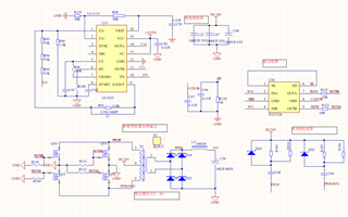
Input: DC 12V (12V7AH battery)

Output: DC 110V

Full bridge field-effect transistor: IRF3205

Transformer turn ratio: Np: Ns (7:80)

PWM frequency: 15KHZ

Inductance(L3): 1mH

Capacitance(C58): 68UF/400V

The principle diagram of the push-pull converter for full bridge rectification is as follows

Some problems is as follows:

There are two uses for personal understanding error amplifiers

1.operational amplifier

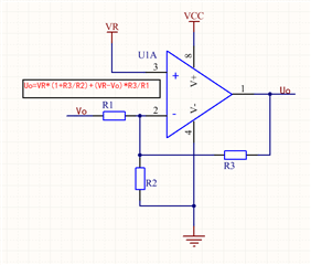
So Uo=Uo=VR*(1+R3/R2)+(VR-Vo)*R3/R1

2.comparator

R3=100K ,When the output voltage of the push-pull converter is divided by R1 and R2 resistors and greater than VR, the error amplifier output is low, and the PWM duty cycle of UC3525 is zero

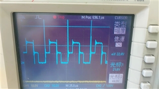
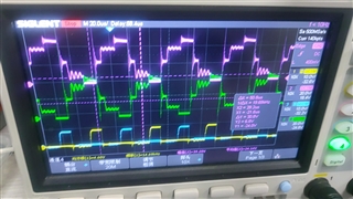
Through testing, it was found that the output voltage of the first type of push-pull converter meets the requirements when it is unloaded, but when it is loaded, the Vds waveform is not good and the efficiency is low

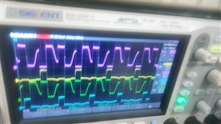
On the contrary, according to the second connection method (comparator), its loaded Vds waveform is good and efficient

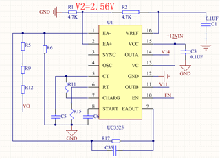
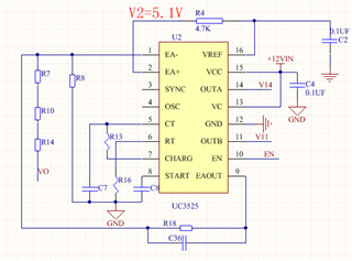
Can the voltage at the 2 pins (EA+) of the UC3525 chip be taken as about half of the reference voltage of 5.1V?

What is the impact of voltage 2.5V and 5.1V at pin 2 on the entire converter?

Limited English proficiency, please forgive any errors

My ultimate goal is to figure out whether the error amplifier is used as an operational amplifier or as a comparator. What is the impact of different reference voltages at the two pins of the error amplifier on the output voltage?

Thank you!

  • Hi,

    These are amplifiers. when you make them with close to open loop, they behave similar to voltage comparator but their comparison speed not as fast as a true voltage comparator. In your case, R3 = 100k, the behavior is more towards to like a comparator. 

    When design it as an amplifier, you would need to design with compensation (feedback path along with R3) with integral effect - without an integral effect, and also if the R3 selected is to make its close loop gain small, then the amplifier output is in proportion to the the input so you can only get the output with the error design in your circuit.

    So in your first type, you need to introduce the integral effect. You can search the internet by type -2 or type -3 loop compensation to help you move on.

  • Thanks for your detailed reply

    When I connect a capacitor (100PF) at both ends of R3 in parallel, the push-pull converter can carry load (with an output voltage of 75V and a load resistance of 50 ohms). After running for 5 minutes, the heat sink temperature of the four MOS tubes is at 50 degrees Celsius. However, when I connect the inductive load, the Vds waveform is chaotic and the efficiency is low. The four MOS tubes will burn out within two minutes. When the push-pull converter outputs a parallel diode (10A10), I think it is the current direction of the secondary side of the rectifier bridge that affects the Vds waveform of the primary side? So I would like to inquire if the voltage and current of the secondary side have an impact on the primary side drive and what is the impact on the Vds of the MOS transistor of the primary side?

    Thanks

  • What is the voltage range at pin 2 (EA+) of UC3525? Why do we almost always obtain 2.55V by dividing the voltage of two resistors with equal resistance values on the 16 pin (VREF) of UC3525 in actual products?

    May I ask if the voltage of EA+cannot exceed 2.55V or if it has a negative impact on the entire push-pull converter?

    VEA+=2.55V

    VEA+=5.1V

  • The same circuit only replaces the battery of the push-pull converter with 2 12V (12V7AH), the transformer turn ratio is changed to 3:52, and the output Vo target value of the push-pull converter is 350V. The Vds waveform changes, and the load (resistance 200 ohms). The overall efficiency of the push-pull converter is low, and the heat sink temperature reaches 90 degrees Celsius. The diode of the rectifier bridge will break down (MUR460), only changing the input voltage, Why is the efficiency low and even diode breakdown when using a push-pull transformer and output voltage?

    The VDS waveform in Figure 1 shows that the efficiency of the push-pull converter reaches over 85%

    The Vds waveform in Figure 2 shows that the efficiency of the push-pull converter is less than 50%

    What factors cause different VDS waveforms? What are the ways to improve?

    Thanks a lot

  • Hi,

    On these questions:

    "What is the voltage range at pin 2 (EA+) of UC3525? Why do we almost always obtain 2.55V by dividing the voltage of two resistors with equal resistance values on the 16 pin (VREF) of UC3525 in actual products?"

    It is a convenient way to get the EA+ from VREF = 5.1V, and it is better to center the EA+ at half of VREF as internally the amplifier is biased with 5.1V

    "May I ask if the voltage of EA+cannot exceed 2.55V or if it has a negative impact on the entire push-pull converter?"

    EA+ can be slightly higher or lower than 2.55V but internal amplifier is biased by 5.1V so it is better to center EA+ at 2.55V. 

    I will answer other questions separately. 

  • Hi,

    On the below queations:

    "I think it is the current direction of the secondary side of the rectifier bridge that affects the Vds waveform of the primary side?"

    One possible is heavier load causing unstable operation. Another is heavier load current causing higher leakage spikes to damage the MOSFETs. Usually you need check the waveforms of Vds of the MOSFETs to make sure the voltage spikes not exceeding the MOSFETs Vds rating. Also you need to measure Bode Plots to make sure enough gain and phase margin. 

    "So I would like to inquire if the voltage and current of the secondary side have an impact on the primary side drive and what is the impact on the Vds of the MOS transistor of the primary side?"

    Yes, as described above.

  • Hi,

    Is below the MOSFET Vds waveform? Are these spikes over the MOSFET Vds rating?

    What are the waveforms below? Can you label each waveform?

    What is your transformer specs?

  •  spikes nearly the MOSFET Vds rating

    Waveforms order:

    Q10:VDS,VGS

    Q13:VDS,VGS

    Two MOS transistors drive waveforms with a phase difference of 180 degrees

    Transformer turn ratio:3:50(Np :Ns)

  • Thank you. I understand

  • Thank you. I understand

  • Hi,

    For the waveforms, what were their operation conditions, Vin, Vout, Iout?

  • VIN:+24V(TWO battery)

    Vout:DC310V

    Iout:0.7A

    After replacing the new transformer, the efficiency of the push-pull converter has increased to over 90%, and the VDS waveform has greatly improved. Can you please advise which parameters of the transformer will affect the Vds waveform? What conditions should be paid attention to when designing a push-pull transformer?

    May I ask if there are any examples of push pull converters? Where can Some of Snubber Circuit be added to a push-pull converter? How can the RCD (including RC, CD, RD, etc.) Snubber Circuit ensure that the resistance does not burn?

  • Changing the output voltage (from 75V to 200V, that is, only changing the resistance value of the UC3525 sampling resistor) results in a completely different VDS waveform of the MOS transistor? Why is this?

    Figure 1 (Vout 75V  VGS VDS wavform)

    Figure 2(Vout 200V  VGS VDS wavform)

    两者效率均在90%以上

    Both have an efficiency of over 90%

    Why are the VDS waveforms different between the two? Is it the output voltage that affects the VDS waveform?

  • Hi,

    Yes, the secondary side status affects the primary side along with the transformer. I think you can find why the waveforms in particular shapes by also adding waveforms of the transformer secondary side winding waveform, or the waveform of D9 and D22.

    I will look for if any references exist that can help snubber design,

  • Thank you very much for your help

  • Hi,

    Snubber design in push pull converter.

    There are quite a few on internet, for example, some below. You can search on to get, "push pull converter snubber design"

    CCFL Push-Pull Snubber Circuit | Analog Devices

    RC snubber for push-pull DC/DC converter | Electronics Forum (Circuits, Projects and Microcontrollers) (electro-tech-online.com)

  • Thanks a  lot