This thread has been locked.
If you have a related question, please click the "Ask a related question" button in the top right corner. The newly created question will be automatically linked to this question.
The output of the push-pull converter is used as the bus voltage to supply the single-phase inverter H-bridge (i.e. realizing the conversion of DC24V to AV380V, 50HZ)。The inverter output adopts an open-loop method
The output voltage of the single-phase inverter is AC380V. The four MOS transistors powered by the single-phase inverter H-bridge are driven by the PWM of TIM1 in the AT32F415 microcontroller. The H-bridge circuit diagram does not provide it. The current problem is:
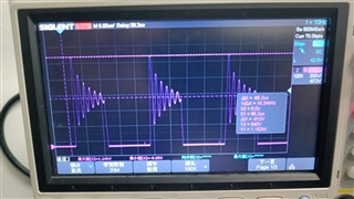
When inductance L3 is present, when the inverter output carries a load of 500W, the peak voltage of MUR8100 may sometimes exceed 1KV, causing MUR8100 to explode. What is the cause of this voltage peak? How to eliminate voltage spikes?
When the inductance L3 is removed from the push-pull full bridge rectifier output, the MUR8100 bears a peak voltage of about 600V when the inverter output is loaded
May I ask why inductance causes an increase in peak voltage?
Thank you!
Input: DC 24V (Two 12V7AH battery)
Output: DC 550V
Full bridge field-effect transistor: MUR8100
Transformer turn ratio: Np:Np: Ns (6:6:168)
PWM frequency: 30KHZ
Inductance(L3): 10mH
Capacitance(C58,C63): 68UF/400V
The principle diagram of the push-pull converter for full bridge rectification is as follows figure1
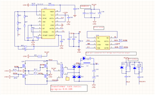
figure1
Iiujun,
I'm not sure what is the purpose of the parallel resonant circuit formed between (D2+C64)//L3? Consider to remover D2+C63. Also for the two HV output capacitors stacked in series, consider to add balancing resistors which means high value resistor in parallel with C63 and another of the same value in parallel with C58. Check dead-time directly at OUTA, OUTB from the UC3525 and compare to the dead-time observed at VGS for each corresponding MOSFET in bridge. Measure the leakage inductance of the transformer, when out of the circuit, and make sure it is reasonable (rule if thumb is less than 1% Lmag).
For the compensation, measure the open loop response of the converter with a network analyzer and compensate accordingly. For VMC you should be considering a Type 3 comp network. For help to model the control and verify your push-pull power stage I recommend to download the free TI Power Stage Designer and read the accompanying application notes.
Regards,
Steve
D2, C64, L3 are used to eliminate the peak voltage of the rectifier output of the converter
Hi steve,
Hi Liujun. Steve is OOO for a while, so I've asked Hong to respond. Please excuse the delay during this transition.
Ray
Hi,
Can you please provide the waveform of the rectifier voltage and show the peak voltage you mean between with and without D2, C64, and L3? So I can understand what you are asking?
Figure 2 shows the voltage waveform of D22. Why does oscillation occur? How to eliminate oscillations?
Figure 2
May I ask what kind of absorption circuit is added to the primary winding of a push-pull converter? What kind of absorption circuit is added to the secondary side of a (RC, RD, or RCD) transformer? (RC or RD or RCD or dual CDD)
May I ask where the absorption circuit is located?
Before the rectifier bridge or each diode needs to be added?
Thank you!
Hi,
D22 oscillation is due to the transformer leakage inductance and parasitic capacitance. D2 can also join the D22 oscillation so if adding some resistance in series with D2 can help attenuate the oscillation. But I am not understanding why you need D2 and C64 if L3 is for output capacitor. I think D2 and C64 should be removed. You can add R-C in parallel with D22 to reduce its ringing. Your layout should be improved to help if you can shorten the parasitic capacitance and shorted the length from the transformer to D22.
The secondary rectifier snubber can be done on each diode or on an arm, i.e., on the left of L3 to GND.
The snubber on the primary side to attenuate the Vds ringing of the MOSFETs such as Q10 can also use R-C. You can also try to add a diode from transformer 3 (anode) to 4, and 5 (anode) to 4 to see if the ringing can be reduced.
The first critical step is to reduce your transformer leakage, and also improve your power stage loop area, make thicker traces to help reduce the ringings..
Hi Hong
Adding D2 and C64 is to reduce the voltage spike of the rectifier diode in the rectifier bridge. After experiments, it was found that after removing L3 (including D2 and C64), the voltage spike of the inverter output with load is lower than that
Hi,
D2 and C64 will introduce high frequency noise to the output as C64 provide low impedance to high frequency. So it is not good to use D2 and C64 for the rectifier snubber.
Hi,
Standard push-pull boost full bridge converters all have output inductance. When can the output inductance be removed?
What are the requirements for the output capacitor when removing the output inductance? At present, no books have been found to remove the output inductor. Is there any book that mentions removing the output inductor?
Thank you!
Hi,
Typical applications are when each push-pull MOSFET duty cycle setup at 50%, and fixed input voltage and fixed output voltage. The output capacitors are mainly depending on the dead time during which how much Vout dip your application can tolerate based on your load condition since during the dead time the capacitors will keep providing energy to the load so discharge the capacitors then causing dip. So you need to know what dip is acceptable then estimate the energy to the load to decide the capacitors.