Other Parts Discussed in Thread: TMS320F28035
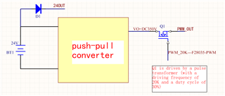
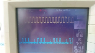
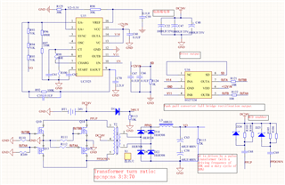
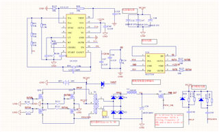
The input voltage of the push-pull converter is DC24V ( two 12V batteries). DC24V is output to external devices through a diode to supply power. When the push-pull output Vo (DC350V) passes through the MOSFET(Q1)
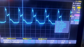
and outputs at 20KHZ (with a duty cycle of 30%), there is high-frequency interference when there is no load on 24OUT.
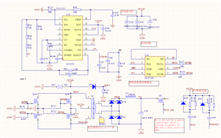
The schematic diagram of the push-pull converter is shown in Figure 1
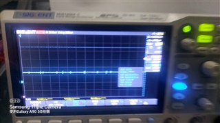
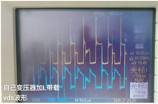
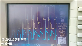
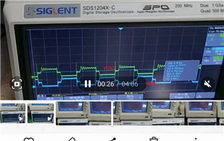
The schematic diagram of the output Vo of the push-pull converter through MOSFET (Q1) is shown in Figure 2

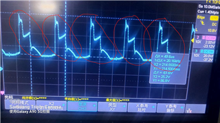
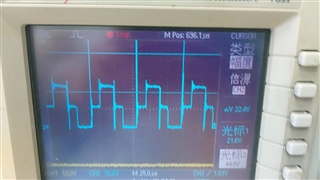
The schematic diagram of DC24 output through D1 is shown in Figure 3
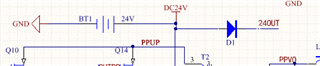
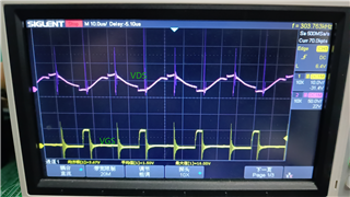
There is high-frequency interference waveform on 24OUT, as shown in Figure 4
What is the source of this interference? How to eliminate this interference?
Thank you!