This thread has been locked.

If you have a related question, please click the "Ask a related question" button in the top right corner. The newly created question will be automatically linked to this question.

LM5113: High inrush current transient

Part Number: LM5113
Other Parts Discussed in Thread: LMG1205,

Hi together,

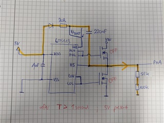
we usethree LM5113 in our 3-phase inverter design with EPC2022 GAN-Fets. We do not use any gate-resistors neither for turn-on nor turn-off.
Furthermore we don´t have any filter elements at the gatedriver inputs.
Each Gatedriver is decoupled with 1uF placed direct to the VDD and VSS pins. External Bootstrap-Diodes with 20R series resistor are also placed accoriding to the actual datasheet.

The initial situation at the beginning is as follows: The three gate drivers are supplied from the same 5V rail. Even the bootstrap capacitors are already fully charged since both PWM inputs are driven low and the switching node is high impedant. Bootstrap capacitors are charged, because we have a voltage divider for measurement purpose at each switching node. So bootstrap capacitor charges with enough time over this path when VDD is provided.

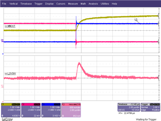
We discovered, that when we start commanding the driver with PWM pulses (High-Side ON, Low-Side OFF) the first high-side-ON pulse is somehow ignored from the driver. That behaviour somehow
makes sense to me, since the bootstrap capacitor might not be charged already. So no switching at the output for the first pulse pattern. So far so good.

With the second PWM pulse pattern (High-Side OFF, Low-Side ON), the switching node is driven low, which is fine. Then everything works fine.

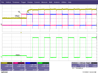
The one thing I am wondering about is, that at the moment when we first time turn the Low-Side ON, the three gatedrivers draw a very high inrush current (3A for 300ns) from the 5V rail even they are decoupled by 1uF MLCC (see picture attached). It looks like that there has to be charged some capacitance or so.

So since the bootsrap capacitor is already charged and the total gate charge of the EPC2022 is just about 13nC, where does the high inrush-current (just at the first Low-Side-ON pattern) come from or flow to?


Would you say this behaviour is normal?

Current drawn by thre LM5113 turning on the Low-Side at the same time. Timescale 500ns/DIV, Vertical: 1A/DIV.

Thanks in advance.

  • Hey,

    Thanks for your question regarding the LM5113.

    It is normal to see a spike in Vdd when HO or LO go high, this is needed for the driver output current to the FETs. When the low-side is turning on, Vdd is having to recharge the bootstrap capacitor as well as drive the low-side gate current. Overall, this is an expected behavior.

    Let me know if you have any further questions.

    Thank you,

    William Moore

  • Hi William,

    thanks for your response.

    But the bootstrap is already charged before we are sending any PWM pulses and the first high-side switching is ignored from the driver? So the charge needed should only be for turning on the low-side.
    Is there any internal logic, which ignores turning on the high-side when it has not seen a low-side pulse before?

    Best regards,

    Clemens

  • Hey Clemens,

    How are you measuring bootstrap capacitor voltage?

    It needs to be measured HB-HS because if you are measuring HB-GND, you are not sure of if the capacitor is actually charged. This is because the HS node can float up to a higher voltage level to where the capacitor doesn't charge but to a couple volts and so it has to be charged and therefore the first high signal would get ignored.

    Can you show me or tell me more about your topology?

    The topology determines more about the status of HS in this case.

    Let me know your findings on this and if you have any further questions.

    Thank you,

    William Moore

  • Hey William,

    thanks for your advise to measure the bootstrap voltage with differential probes. At first it was a single ended measurement.
    As it turned out, you were right. Even if the switching node is pulled down by a 151k resistance path, the node is still floating at about 2.5V and the bootstrap capacitor was only charged at 2V. This was the reason why the first HS-PWM pulse is ignored.

    I was assuming a current path like this. But maybe the 151k are to week to pull the switching node down when all drivers are off.

    We also generated some waveforms where we measured the input current of three LM5113 getting the same PWM pattern simultaneously. We put 2uF decoupling capacitor at each VDD pin next to the chip:

    We saw a current peak at about 1.5A. This is needed to charge up three bootstrap capacitors of 220nF (2V up to 4.5V) and to turn on three LS FETs (EPC2022) at the same time. The current sourced from the decoupling capacitors can not be seen within that current waveform.
    Would you say that this is plausible? And can you tell me something about the internal bootstrap path?
    Does the major current uses the external current path to the bootstrap capacitor when the components are chosen acording to the datasheet? Why did you decide to recommend external bootstrap components at later revisions?

    Best regards,

    Clemens

  • Hey Clemens,

    Thank you for the waveforms and the updates.

    As a reminder, the LM5113 is no longer recommended for new designs as noted on the product page. The LM5113-Q1 is still an active part in the WSON-10 package and the LMG1205 is an active part in the DSBGA-12 packaging.

    When the low-side is driven, the current path would be from VDD to LO. The decoupling capacitors would already be charged and therefore it would be sourcing current from there and VDD. So, with a peak source current value of 1.2A for the driver as well as needing to charge the bootstrap capacitors, a peak value of 1.5A is reasonable.

    As for the internal bootstrapping circuitry, specifically the diode, this diode is not being turned on in this case due to HB being left floating (If that is how you have it set up). So, due to this the current path is through the external diode to the high side and for the low-side, the current path is VDD to the driver.

    I cannot speak specifically as to why the external diode was recommended on this device as that was before my time with this product line, but the LMG1205 is an option if an integrated diode is something that you need.

    Let me know if you have any further questions.

    Thank you,

    William Moore

  • As for the internal bootstrapping circuitry, specifically the diode, this diode is not being turned on in this case due to HB being left floating (If that is how you have it set up)

    Sorry for that, I just forgot to draw the line. Replaced the picture above for the others.

    Thanks a lot for your help William. I really appreciate it!

    Best,

    Clemens