This thread has been locked.

If you have a related question, please click the "Ask a related question" button in the top right corner. The newly created question will be automatically linked to this question.

UCC5350: if need extra self boost circut?

Part Number: UCC5350
Other Parts Discussed in Thread: SN6501,

Dears:

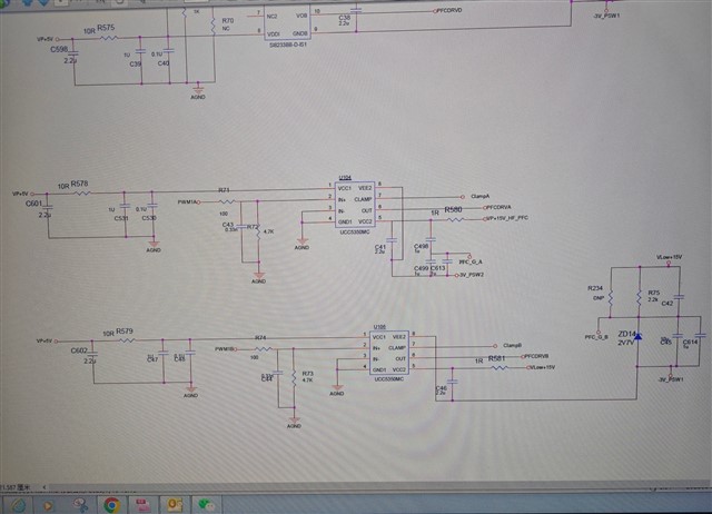
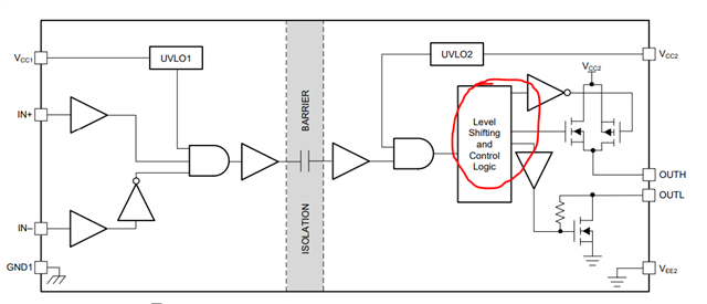
customer use SI8233BB-D-IS1, they want to use UCC5350M-Q1 to replace it. Could you please help check if UCC5350M-Q1 need extra self boost circuit ? If not, Could you please help introduce UCC5350M-Q1's working method ? Thanks.  

  • Hi Haiwen,

    Our expert is out of office due to Thanksgiving US holiday. We'll respond to you once they're back after the break which is 11/27/2023.

    Best,

    Pratik

  • Hi Haiwen,

    Sorry for the delay. What do you mean by self-boost? Is this the same thing as a bootstrap power supply circuit? Here is an application note that discusses the design of a bootstrap supply: https://www.ti.com/lit/an/slua887a/slua887a.pdf . Another possibility is to use an isolated power supply, such as a push-pull driver like the SN6501 and a small transformer, followed by an LDO.

    The UCC5350/90 can be used without the dual channel driver, since it is itself an isolated gate driver. If you simply want to boost output current, you might consider using a BJT totem pole instead, (using a composite/Sziklai PNP). Two isolation barriers seems excessive.

    Best regards,

    Sean

  • Hi Sean:

    Customer want to know the high side MOSFET 's gate voltage comes from level shift or other circuit ? 

  • For the PMOS on the left side of the pull-up network, so no level shifting is needed. The gate is attached to ground. For the NMOS on the left, its gate is attached to Vcc. It will turn itself off once OUTH reaches Vcc-Vth_n. 

    Vcc2 still has to be 12V-18V above the Vs of the Power FET. This will change whether the high-side switch is ON or OFF, and it must float on top of the switch node voltage. That is why the high side gate driver requires either a bootstrap supply or an isolated bias supply, which can float on top of the switch node voltage.

  • Sean:

    customer want to know how VCC2 side to lift voltage 12-18V to control MOSFE ON/OFF. They want to know the internal principle of the circuit. Could you please help to explain it to customer ? Thanks.

  • Hi Haiwen,

    Voltage is always defined as a potential between two nodes. Let's make sure to define what each voltage is referenced to. 

    Let's say the high voltage power supply of a half bridge is 100V, and power ground is 0V. There are two NMOS in series, a low-side and a high-side. Vsw is the voltage of the node between the two power FETs. Let's say the power supply to the gate driver is Vee2 =0V and Vcc2=20V. 

    The gate driver will be able to drive the low side gate no problem. Vs of the low side is 0V, and Vg can be brought to 20V.

    However, the gate driver will have a problem driving the high side gate, since Vs of the high side gate is Vsw. If Vsw rises to 20V, Vgs of the high side gate will be 0V.  

    Therefore, the high side needs a different kind of power supply, either a "bootstrap supply" or an "isolated supply".

    In these supplies, Vee2 does not always equal 0V. It is connected to Vsw. Vcc2 is connected to a capacitor charged to 20V w.r.t. Vsw. When Vsw rises to 20V, Vcc2 rises to 20V+20V=40V. 

    Did you just email me a Zhuzhou schematic for review? In that design, a SN6505 push-pull was used to drive a transformer. The primary is connected to 0V, but the secondary of the transformer has its low side connected to Vsw. The power supply will always be able to deliver a 20V Vgs, regardless of the Vsw voltage.

    Best regards,

    Sean