Hi
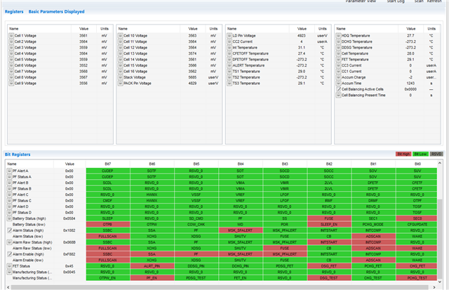
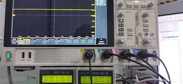
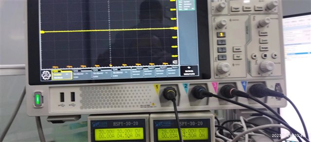
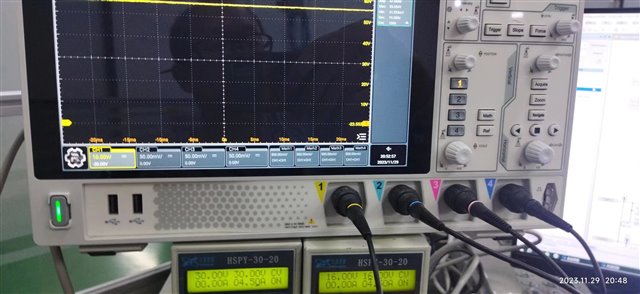
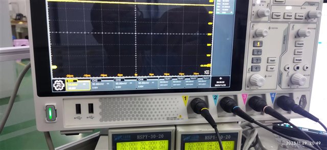
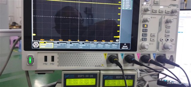
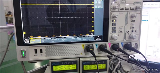
The customer design with BQ76952, after the battery voltage of 16 series is higher than 52V, the output voltage of PACK+ is limited to around 52V.
At this time, the boost voltage of CP1 also drops from 11V to less than 1V.
At this time, the boost voltage of CP1 also drops from 11V to less than 1V. The DSG and CHG are externally cut off, as are the connections between PDSG, PCHG and MOS.
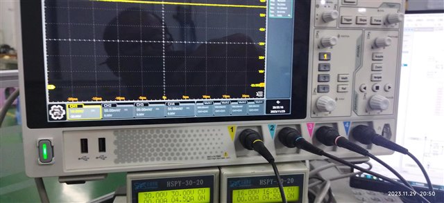
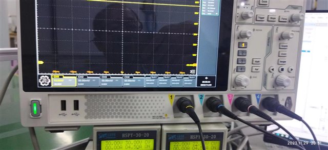
Increasing the capacitance to 2.2uF has no change. In normal mode and test mode, after initialization, the voltage of CP1 is still nearly 11V before enabling FET, and drops to less than 1V after enabling FET (when the battery voltage is above 52V).
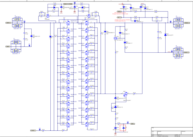
The schematic as below:
Please help check it.
Thanks
Star