Dear TI team,
we are currently having issues with a design that uses the LM5123.
We are using the LM5123 as a step-up converter, going from 10-32 V input voltage to 32 V output voltage. We originally had some issues with ringing on the low side FET (see related post), which we were able to mitigate using a snubber. However, another problem has occurred.
When providing a low input voltage (e.g. 10 V), we get excessive heat from the low side FET, even with light or no load on the output. This behavior decreases when using higher input voltage.
Our preliminary findings seem to indicate that the LM5123 is violating the dead time for the low side FET, and is actually switching the low side FET on while the high side FET isn’t fully closed yet, thus creating a short between VOut and GND.
As a first measure, we added a gate resistor of 2 Ohms to the low side FET to delay the switching of the FET, but this only slightly improves the situation.
We also tried to change the FETs, we originally used the Nexperia PSMN3R2-40YLD, we also tested the ONSEMI NTMFS5C670NLT1G (which is used in the evaluation board of the LM5123), since we feared out original FET might have a too high of a gate charge. However, this also didn’t improve the situation.
Additionally, we have a snubber (2.2 Ohms, 1.5 nF) in parallel to the FET, to mitigate EMC issues. However, the behavior doesn’t seem to be influenced by the snubber, as it is similar without the snubber.
As I understand, the LM5123 has an adaptive dead-time, which actually measures the voltage of the high side FET before switching on the low side FET. Might that be an issue in our design?
Do you have an explanation for the behavior? Is there anything that could improve the situation?
Best regards
Felix
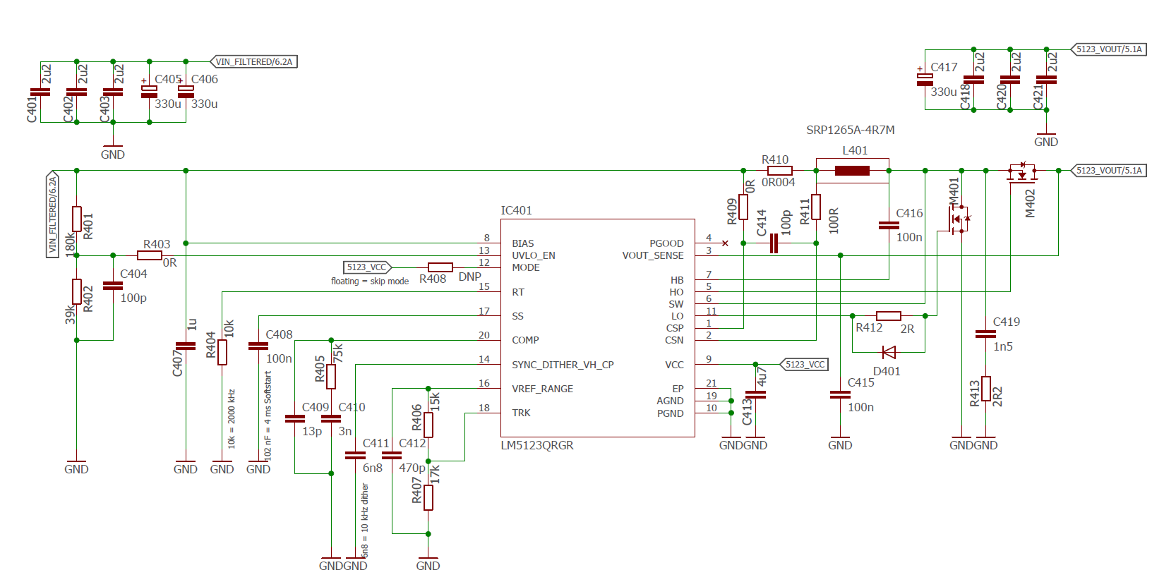
Schematic: