This thread has been locked.

If you have a related question, please click the "Ask a related question" button in the top right corner. The newly created question will be automatically linked to this question.

TPS61023: Output voltage increases with closeness of finger....

Part Number: TPS61023

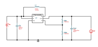
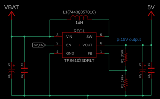
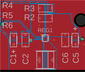
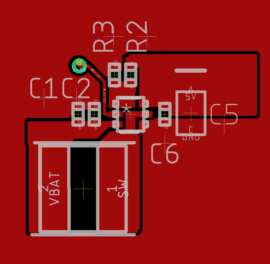
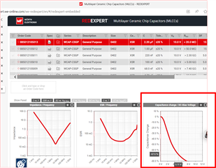
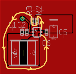
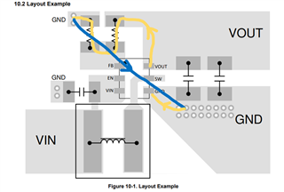
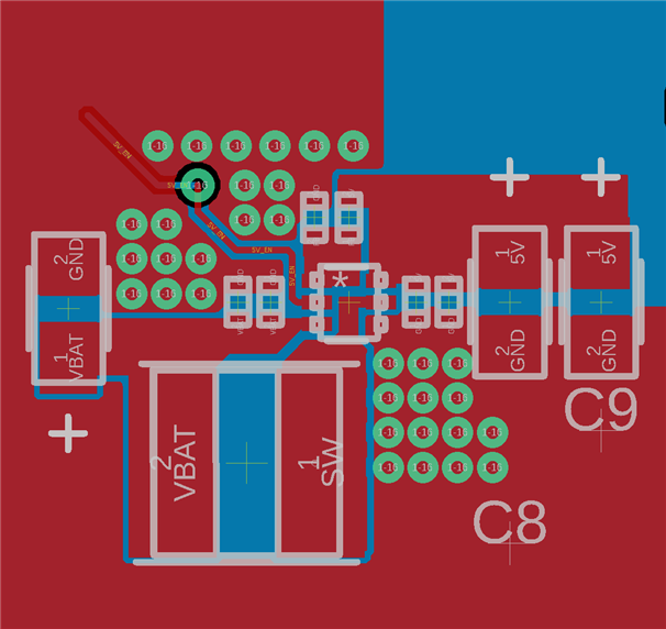
So I built this circuit using webench. I've attached the SCH & PCB. It's a simply 2 layer PCB, not much going on.

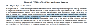
The circuit outputs 2.15V as advertised. Currently I have a 200mA load connected, everything is hunkey dorey. When I bring my finger close to the chip itself, the voltage begins to increase. The closer my finger, the higher the output voltage until my finger touches the chip and it fries and creates a dead short from VIN to GND. I've done this twice! On the third time, I added the feed forward capacitor (as recommended on webench) of 1pF as a "what else to do" solution. My logic was stray capacitance from my finger was influencing the FB pin somehow (hence the increasing output voltage). The same thing happened. What on earth is going on here? What do I even try to start troubleshooting?

  • Hi Marcie,

    I'm not sure what influence your finger has on the IC since I don't know your ESD measure. But I think you can optimize your poor layout to avoid some problem. Please view this application note and send me your optimized layout so that I can review it:

    ti.com/lit/an/slvaes4/slvaes4.pdf?ts=1702259022389&ref_url=https%253A%252F%252Fwww.ti.com%252Fsitesearch%252Fen-us%252Fdocs%252Funiversalsearch.tsp%253FlangPref%253Den-US%2526searchTerm%253D61022%2Blayout%2526nr%253D60

    Also, the problem may be generated by parasite capacitance between FB and ground. Use smaller footprint on R2 and R3 and place the footprint close to the IC so that the FB area can be reduced. And do not use such thin wires on a power path like you did on the 5V and Vbat net.

    Try copy the EVM layout or datasheet layout example if you did not employ a trained layout engineer.

    Best Regards,

    Travis

  • Thank you for linking the document, it was very helpful. After a thorough read, here is the updated layout. 

    Vin and Vout have not been routed, so they are surrounded by the GND pour. They will get beefed traces from the previous layout. 

    C1 = C6 = 10uF, C2 = 0.1uF, C5 = 22uF.

  • Hi AJay,

    The layout is good. Here's my comment on some details:

    • Is C5 a ceramic cap? Electrolytic capacitors has bad performance on filtering Vout ripple because of its large ESR, so usually for low voltage applications we apply only ceramic caps on the output.
    • C1 is not enough for input capacitor. Because of the saturation characteristics of ferroelectric materials, ceramic caps has DC bias effect which will massively reduce its effective capacitance when a DC-voltage is applied. The smaller footprint is and the bigger the capacitance is ,the stronger the DC-bias loss will become. So 0402 10uf will suffer a lot of DC bias loss
    • Also, if you're testing the board through long wires:
    •  Since you're using 2 layers boards, we recommend pouring the bottom layer with GND ,too. Otherwise some path will take a long way to return and form a loop antenna. Which will make FB more vulnerable to EMI.

    Best Regards,

    Travis

  • Travis,

    The bottom layer will be a complete GND pour. I'll make sure to add vias to both input side GND plane and output side GND plane so that the loop you are drawing is exactly as shown in the layout 10.2 example. Can you please explain what this loop from VOUT to GND is? 

    C5 is a 22uF tantalum capacitor. In my initial drawing I had a 22uF tant on the input as well, but it was too large to get close to the input pin :). Can you recommend general input/output caps? Should I keep a 0.1uF cap as close to the input as possible? It's recommended in the document you linked, but nowhere else.

  • Hi AJay,

    1. This is the FB sensing loop.
    2. For boost topology, Vout is more critical than Vin. As tantalum capacitors usually has big ESR, you can have it on the input and don't need to place it so close to input pin. The parasite inductance impedance is going to be smaller than ESR and therefore could be neglected.
    3. Putting a 0.1uF cap as close to the input as possible is good. You can keep the design.
    4. Input/output caps recommendation: You can copy the BOM on the EVM user guide: TPS61023EVM-052 Evaluation module user's guide

    Best Regards,

    Travis

  • Travis,

    Thank you so much! I'll make sure to come back here if the new version has any troubles.

    Cheers,

  • Travis,

    After consideration, this looks like it meets previously stated criteria. Ground loop has been reduced to across the chip with vias and ground pours. The vias are as small as my fab house will allow without crazy surcharges. The loop you've previously shown should now cross the device as shown in the EVM datasheet.

    Input bulk cap = 47uF tant, 10uF & 0.1uF ceramic 0603 X5R.

    Output, 22uF ceramic 0603 X5R, bulk 47uF tants. I'm very tempted to add a 0.1uF on closest to the output before the 22s. Most circuits I see have one there. 

  • Hi AJay,

    This layout is good. I advise changing Cout to 0.1uF + 22uFx2 and remove the output tant. As I mentioned before, ceramic with small footprint and big capacitance will suffer a lot of DC-bias loss. I don't know your BOM but from my experience, 22uF 0603 will have about only 5uF effective capacitance under your 5.15V output. So I recommend 22uFx2.

    Other parts are good.

    Best Regards,

    Travis