This thread has been locked.

If you have a related question, please click the "Ask a related question" button in the top right corner. The newly created question will be automatically linked to this question.

LM34936: High voltage application

Part Number: LM34936
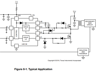
Other Parts Discussed in Thread: LM5176, , LM2105, CSD19502Q5B, LM5108

One question regarding the thread of Tyhran with the same title from about 3 months ago;
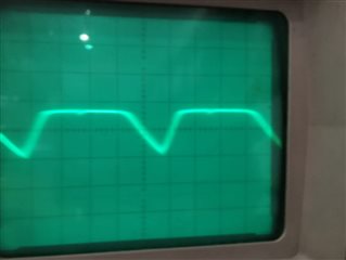
Would the circuit shown thre really work? Although there was no negative comment on that topic I wonder whether the connection of SW1 and SW2 (and Boost1/2, too) to GND (to VCC) instead of to the switching nodes would work. We built up a respective prototype after this circuit and there was no output switching signal from the IC. There is no deeper explanation about the functions of SW1,2 and Boost1,2 in the datasheet, so we would really need the feedback of a TI expert.

  • Hi Oliver,

    as already mentioned yesterday please apply at VIN the min voltage to get the controller enabled VIN > 2.5V

    When referring to another thread please add the link to the thread as a reference or just add the question to the existing thread if it is discussing the same topic.

    Best regards,

     Stefan

  • Please find below the link:
    https://e2e.ti.com/support/power-management-group/power-management/f/power-management-forum/1277516/lm34936-lm34936-with-high-voltage-application?tisearch=e2e-sitesearch&keymatch=lm34936#

    We assume that the circuit won't work with these connections of SW1,2 and Boot1,2 and the low drive currents to the external gate drivers instead of the MosFet gates. What do you think?

    Could you recommend another circuit and IC as gate drivers for our application? The main problem is our high input voltage of up to 85V and output of up to 56V. 

    Best regards,

    Oliver

  • Hi Oliver,

    the generation of the GND related control signals for the high side MOSFETs on the LM5176 with connecting SW1 and SW2 and applying external voltage to BOOTx will work. 

    There is just one limitation during the Softstart phase that the low side BUCK MOSFET will not be enabled and the current will flow through the body diode of the MOSFET. So higher losses in that phase will appear.

    Best regards,

     Stefan

  • LM5176 ... did you mean LM34936 (this is the IC we are using)?

  • HI Oliver,

    you are right: it is for the LM34936.

    Best regards,

     Stefan

  • Ok, thanks. Could the soft start behaviour of the IC affect the complete start-up behaviour and thus lead to a non-working (non-switching) state?
    Best regards, Oliver

  • Hi Oliver,

    I am not aware of any other limitation then the one I described above.

    Do you still see an issue - even with a voltage level applied at VIN?

    Best regards,

     Stefan

  • Hi Stefan,

    we found a layout problem on the board which was resolved. Now the circuit is running without basic problems, incl. a proper switch-over from boost to buck.

    But we have another substantial problem: The signals at the input high-side Mosfet are looking very poor, rising+falling edges are very sloping. This curve is found at the Mosfet gate and source (= out new "SW1") but also at the gate driver output of the LM34936 (HDRV1). However, the signal looks much better without an input voltage applied, then it's almost rectangular. Ths other signals, especially at the output Mosfets are ok. With a load of about 40W the signal forms iare not really changing, the input Mosfet gets very hot in a short time. Without load the quiescent current is much too high (about 250mA @ 20Vin and 40Vout). 

    Do you have an idea what could be our problem? Maybe wrong cap or resistor values at the slope and comp inputs?

  • HI Oliver,

    thanks for the update.

    To confirm this waveform is measured on the high side BUCK MOSFET between Gate and Source - right.
    (Can you try to get the picture better and also add Time and voltage division?)

    So this would be the drive capability of the LM2105?

    What is the type of the MOSFET you are using? What is the Gate Capacitance?

    How does the BST voltage look like?

    Best regards,

     Stefan

  • Sorry, we don't have a better photo, board is defect now. Oszi parameters were 5V/div (0V line is the 2nd line from bottom, so max. voltage is about 18V (=input voltage). And 2µs/div in x-direction (about 100kHz).

    We use the gate driver LM 5108. MosFet type is NTMFS008N12MC (input, ca. 33nC) and CSD19502Q5B (output, ca. 43nC).

    All ICs are supplied with 12V, so the BST voltage should be like that. 

    Best regards,

    Oliver

  • It's the high side Mosfet at the input (between power input and the inductor). Sorry, we don't have better photos. Oszi parameters are 5V/div (ca. 18V plateau voltage, 0V = 2. line from bottom) and 2µs/div (100kHz).

    Our gate driver is now the LM5108. Mosfets are NTMFS008N12MC with about 33nC total gate charge (input array) and CSD19502Q5B with about 43nC (output array). So these values are still far below the driving capability of the LM5108.

    All ICs are supplied with 12V, BST voltage should be similar, We didn't measure it directly, now the board is defect...

    Best regards,

    Oliver

  • Could you please send me an answer to the open issue with the strange signal slope?

  • Hi Oliver,

    Sorry, I wrongly assumed you would repair the board first and share more details, so thanks for sending the reminder.

    It would be good to get a schematic of the actual board. I am not sure what is still identical to the schematic of the other thread.

    If you see that signal on the HDR1 - then something is not OK. The driver is quite strong and should change the level within a few ns.

    I do not understand this sentence: "However, the signal looks much better without an input voltage applied, then it's almost rectangular."

    Can you please explain that in more details?

    Best regards,

     Stefan

  • Hi Stefan,

    we have used exactly the same circuit as shown before and in the previous thread of Tyhran (same project). Normally the high side input Mosfet should be turned constantly on and the low side one constantly off. However, this is not possible from the fact that the gates have to be supplied with a bootstrap voltage which needs a certain switching pulse. This is what we see without power input voltage (but with operating voltage at the DC/DC IC which is separated from the power input voltage: very short and steep pulses to the high side Mosfet. They turn into the signal with diagonal slope as shown before once an input voltage of e.g. 20V is applied (without load).
    Maybe our missing RC elements between LM5108 gate driver and gates and some diodes as recommended from TI problem could be the problem? (see below)

    Best regards,

    Oliver

  • Hi Oliver,

    I am not the expert for the LM5108 but I am quite sure that the boot circuit (Diode and Cap on HB/HS) will be required on the LM5108 to generate the gate signal for the high side FET.

    If required you can enter a new thread and ask about that with selecting the LM5108 as partnumber - in this case it can be assigned to the right team.

    Best regards,

     Stefan

  • Today we probably resolved the problem by ourselves: We found that the high side gate driver output of the LM34936 doesn't send any switching signal to our external gate driver IC LM5108. The origin for this seems to be the fact that the BOOT pin of the LM34936 is connected to the VCC line and thus always "on". Obviously the IC has an internal detection circuit which evaluates the BOOT signal and controle the internal switching process to the respective driver output: As long as the BOOT pin is "on" there is no need for a driver output signal. When we changed the voltage at the BOOT pin to 3V or less the IC it started switching again at this driver output.
    So we have to find another solution to generate the high side gate driver voltage or to stimulate the IC to send the switching signal.
    However, so we found another issue who should be supplemented in the TI datasheet of the LM34936 (after there was no description about the need of the VIN pin to be connected to an external power supply): The BOOT pin gives an internal feedback signal which is needed to keep the IC switching at the driver output.

  • Hi Oliver,

    i just checked the schematic again which you have added into the other thread and have seen there that the VCC and the BOOTx pins of the LM34936 are connected to 12V. This does violate the abs max ratings of this device. So the device might already been damaged if this was really connected to 12V at this pins.

    Also for VIN the minimum voltage is given:

    Best regards,

     Stefan

  • Hi Stefan,

    there seems to be a difference between the previous circuit and our actual one: in our actual circuit the BOOT pins are connected to the VCC pin and separated from the 12V line which is only connected to BIAS and VIN. So this is not the origin for our problems with the high side gate driver outputs.

    We'll modify the prototype by adding an auxiliary circuit and let you know about the results.

    Best regards,

    Oliver