This thread has been locked.
If you have a related question, please click the "Ask a related question" button in the top right corner. The newly created question will be automatically linked to this question.
Hello,
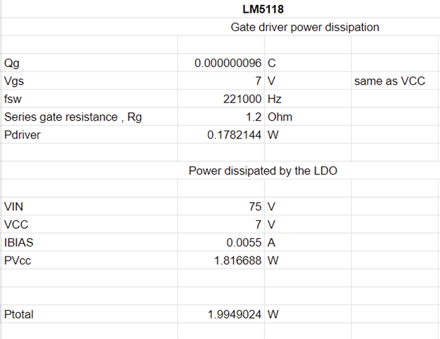
We are considering LM5118 for an application with the following requirements
Vin (min) = 18V
Vin (max) = 75V
Max load current = 3A
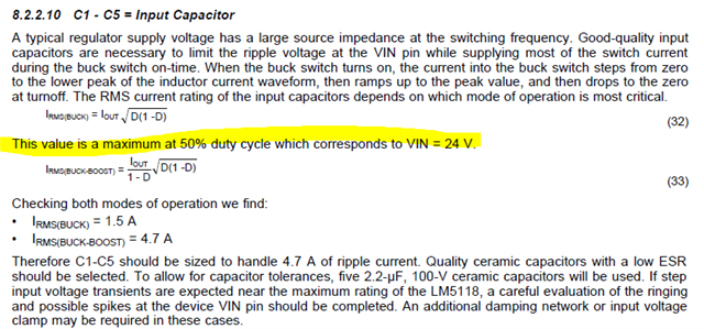
In the datasheet, I came across information suggesting that the RMS current rating is at its maximum at a 50% duty cycle, corresponding to VIN = 24 V. I would like to seek clarification and additional details on this matter to better understand the product's behavior in our application.
Additionally, if there are any specific considerations or guidelines for optimizing performance under varying duty cycles, I would greatly appreciate your guidance.
thanks
Najma
Hi Najma,
for this application example the 50% duty cycle corresponds to 24V - see 8.2.1
VOUT = 12V
D = Vout / Vin => Vin = D * VOUT = 50% * 24V = 12V
To optimize the design you can use the quickstart calculator which can be found on the product page
Note: this is currently not shown but should be available again later today on the product page.
Another option for design optimization is the power stage designer:
POWERSTAGE-DESIGNER Design tool | TI.com
With both tools you can see the impact of component changes and tune the design for your preferred parameters.
Best regards,
Stefan
Hi Stefan
Thanks for the response. I used the WEBENCH power designer available in the product page. https://www.ti.com/product/LM5118#design-development
I'm able to generate a sample design for VIN - 18 - 75V, Vout 24V , Iout 3A and ambient temp 30 degree C . But when I change the temperature to 40 , it says design failed , junction temperature too high. Is it due to the operating temp of components that you are using to generate sample designs ?
Please let me know where can I find the calculations ?
thanks
Najma
Hi Najma,
most properly the calculated losses in the one of the components are so high that it heats up above the limits (e.g. Diode).
When you check the data for the 30 degree you could see the losses and calculate the temp increase of that components.
I have attached the calculator here as it looks like the web update takes some more days.snvu065a.zip
Best regards,
Stefan
Hi Stefan,
I am calculating the power dissipation .
FET part # CSD19532Q5B (one on HO and one on LO). Fsw is 221kHz. The gate driver power dissipation is calculated as Qg*Vgs*Fsw*Rg.
The power dissipated by LDO is calculated as PVCC = (VIN-VCC)*{(Qg*fsw)+IBAIS}
I referred to the following threads
Please let me know if the calaculations are correct.
Hi Najma,
so you would like to calculate the power dissipation of the LM5118 -right?
I can not see the math in the sheet but the formula above look OK.
Best regards,
Stefan
Hi Stefan,
The calculations are as follows
Vin = 18 -75V
Qg = 48nc*2 =96nC (CSD19532Q5B)
Vgs = 7V (same as Vcc)
fsw= 221kHz
Ibias = 5.5mA
Series gate resistance Rg = 1.2Ohm
Gate power dissipation = Qg*Vgs*Fsw*Rg = 0.1782W
LDO power dissipation = (VIN-VCC)*{(Qg*fsw)+IBAIS} = (75-7) * ((96nC*221000)+0.0055)) = 1.816W
The total power dissipation is 1.99W and the calculated temperature rise is 79.76 degree C. Since the PCB has to operate inside a module with worst case temperature of 60 degree C , this will bring the worst case temperature to almost 140 degree C .
Is there a way to limit the LDO power dissipation ?
If the VCCX is biased with 5V ,the LDO won't be operating , correct?
In that case the PVcc = (RDSON)*[((Qg*fsw)+IBAIS)^2] = 0.0034W ( RDSon = 5Ohm from datasheet)
Ptotal would be 0.1782 +0.0034 = 0.1816W
Is this the best option if we want to limit power dissipation and temperature rise ? Please advise
thanks
Najma
Hi Najma,
your calculation looks OK.
For reduction of the loss you can have a lower voltage at VCCX - still higher then 7V to get enough gate signal
e.g. with 10V it would be:
LDO power dissipation = (VCCX-VCC)*{(Qg*fsw)+IBAIS} = (10-7) * ((96nC*221000)+0.0055)) = 80.1mW
But note: the LM5118 has a limitation which requires VCCX only to be supplied after the output voltage has ramped up.
Best regards,
Stefan