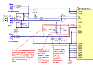
In the Rev. C datasheet Table 8-1 it says "For extreme input ripple voltage cases, connect a 4.75-ohm filter resistor to power input, PIN7, and connect a 10-μF ceramic capacitor from analog VIN PIN 6, to power analog GNDP." but right above it in Figure 8-1 and 8-2 it seems to show this resistor going to pin 6. Am I misinterpreting what is being shown? or is it the text that is tripping me up? Rvina and Cvina aren't referenced by name anywhere so it's confusing.
First I want to understand what the difference between pin 6 and 7 are? I assume one powers the chip and one delivers power to the integrated transformer?
Next for the input filter does the 4.75-ohm connect between pin 6 and pin 7 or between Vin and pin 7? Is the 10μF in addition to the one mentioned at the top of this table entry? and should the ground side of it be closer to pin 5 or pin 8 (both seem to be important for different things as per the Vin entry in Table 5-1)?
And ultimately I want to know what implementing both the optional 330pF and the input filter looks like?