This thread has been locked.

If you have a related question, please click the "Ask a related question" button in the top right corner. The newly created question will be automatically linked to this question.

UCC27282-Q1: Unexpected issue with HO for inverter application

Part Number: UCC27282-Q1
Other Parts Discussed in Thread: UCC27282

Hi,

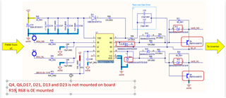
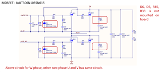
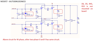
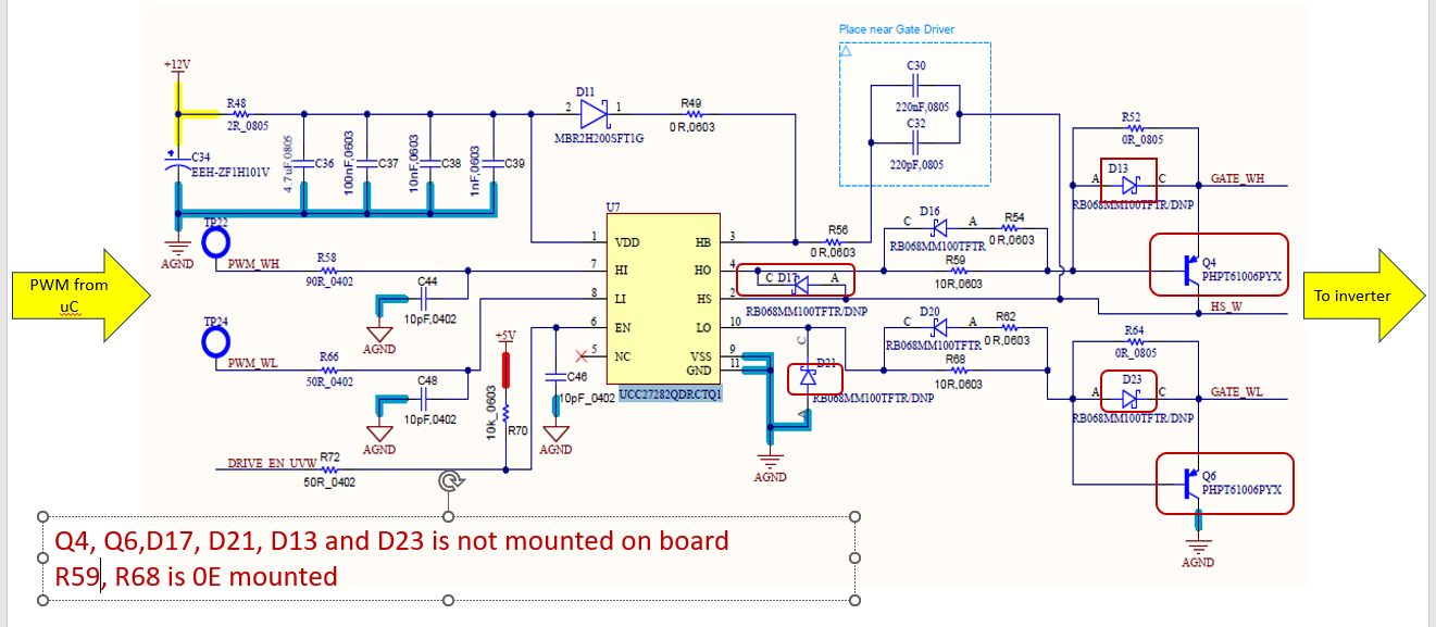
I am using UCC27282QDRCTQ1 to drive the IAUT300N10S5N015 MOSFET for the motor controller application.

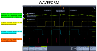
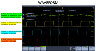
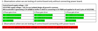
I have tested with 1kHz , 10kHz and 20kHz PWM from microcontroller to Hi and Li pin. 

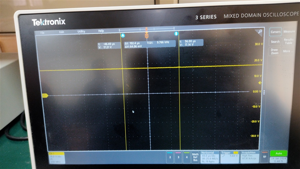
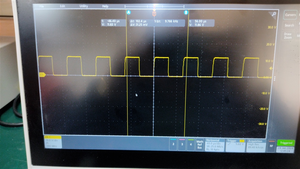
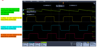
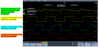
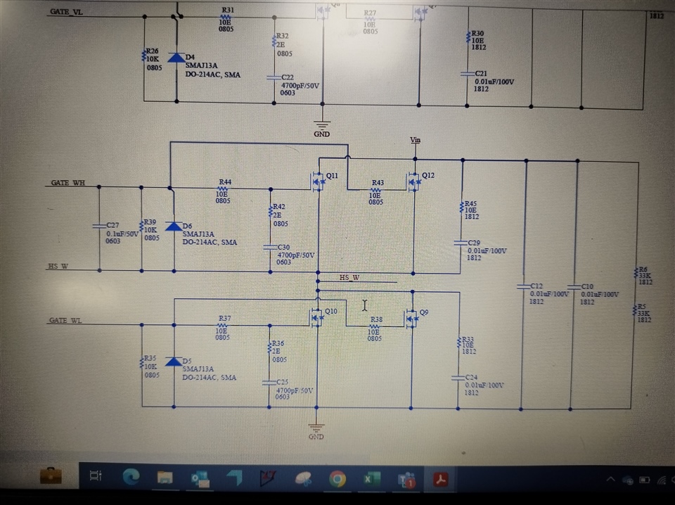
Without connecting MOSFET it's working fine like at LO pin I am getting 12V PWM and HO pin constant 12V high signal. However when I am connecting MOSFET IAUT300N10S5N015. LO PWM is OK at low side MOSFET of all three UVW phase and at HO 12V constant at high side MOSFET of U and V phase but for W phase high side I observed occsilaction at HO. Above test I done without connecting +Ve input voltage to inverter circuit only I have connected ground common with gate driver and microcontroller.

When I am connecting +Ve input voltage to inverter it's getting short with ground.

I have used 220nF bootstrap capacitors..I increased and tested with 4.7uF capacitor then occsilaction resolved but HO voltage increased upto to 17V-18V and when connected inverter +Ve input voltage it's getting short.

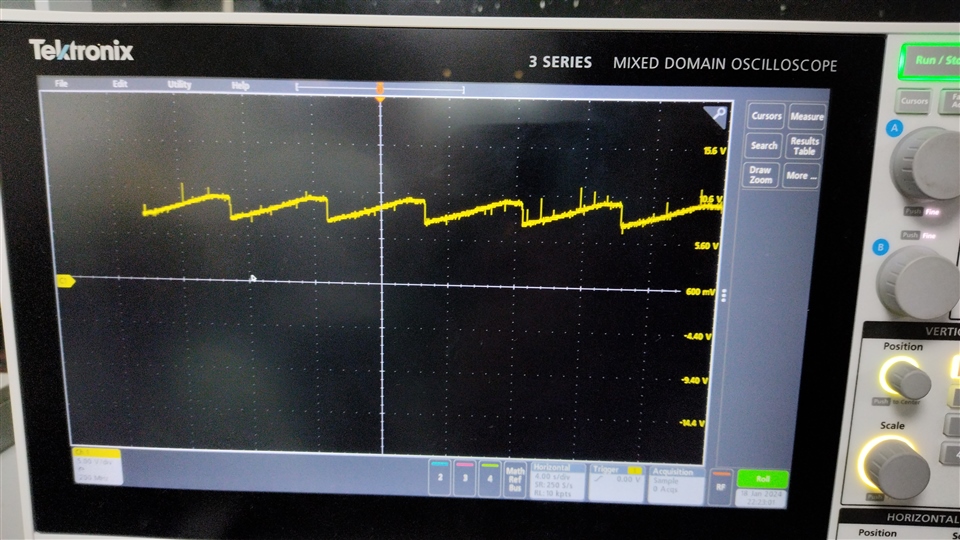
Please guide and support on his priority.

  • Hey,

    Thank you for your question regarding the UCC27282-Q1.

    Can you please clarify what these scope plots are? Are they HO-VSS or HO-HS?

    Please take scope plots with a differential probe of HO-HS and label accordingly.

    Are you experiencing a hard failure on the device or just unexpected outputs?

    I noticed the note to place the bootstrap capacitors near the gate driver, it is also important that the bypass capacitor that is at least 10 times larger than the bootstrap capacitor is placed closed to the gate driver.

    Please label and comment on each of your scope captures so that I know the operating conditions and the measurement being taken.

    Let me know your responses to these questions and if you have any further questions.

    Thank you,

    William Moore

  • I am facing hard failure... shared waveform are for W phase occsilaction and straight 17.6V waveforms are for W phase high side gate waveform....12V PWM is for low side gate of the MOSFET. All waveforms are measured with respect to ground only HO - VSS and HO-VSS.  If you want I will test and share the waveform of HO-HS.

    Which bootstrap bypass capacitor you are taking...C32 or C34 ?

    C34 is 100uF 20% 50V we have placed.

    All three phase U V W has same circuit. I have shared W phase only.

    Q4, Q6 is not mounted in gate driver circuit.

    D5, D6, R45 and R33 is not mounted in inverter circuit.

  • Hey,

    When you see this hard failure, does a replacement of the driver fix the issues temporarily or is the issue consistent with all drivers?

    How many boards have been made and how many are seeing this issue?

    C30 and C32 are the bootstrap capacitors which has a note to be close to the driver, that is good.

    The bypass capacitance (C36, C37, C38, and C39) need to be at least 10 times greater than the bootstrap capacitance. Which with C36 being 4.7uF, that is acceptable. Are these bypass capacitors placed close to the driver? These need to be placed closed to the driver for sourcing currents.

    Please take a waveform capture of HO-HS and label the waveform as well as tell me the operating conditions with which the scope shot is taken.

    The last image in your initial post appears to be operating as intended. What is the condition for that?

    Can you also take waveform captures of HI and LI at the driver with respect to VSS? Also, with these please take captures of HO to HS and LO to VSS at the driver with all 4 signals in the same plot? I want to verify your operating conditions.

    Let me know what your findings are and if you have any further questions.

    Thank you,

    William Moore

  • Hi William,

    We replaced the U phase IC, we are facing issue with all  three U V W drivers.

    5 boards we made and all have same issue.

    When we are connecting inverter circuit with control board  its getting short.

    Hare i have shared W Phase gate driver and inverter circuit , Other U and V phase is the same.

    Please guide.

    Regards,

    Shambhu

  • Hey Shambhu,

    What is connected to HS_W? If there is no output load, then the low-side FET cannot pull this circuit to ground when it is turned on and the bootstrap capacitor will not charge. Therefore the high side will not switch

    Also, the capacitors on VIN (C10 and C12) are too small to help bias the output and source current for the load. I would suggest greatly increasing at least 1 of these to at least 10uF.

    Let me know if you have any further questions.

    Thank you,

    William Moore

  • Hi William,

    There is one correction in previous waveform, the differential probe was set at 500 attenuation(gain). Please see updated waveforms.

    Low side mosfet is switching properly.

    High side mosfet is not switching properly and its shorting the inverter Vin to ground, High side mosfet is not getting OFF properly. 

    HS_W is the W phase for MOTOR, We are testing without connecting motor. 

    Can you please check the boots strap cap value is ok for the mosfet IAUT300N10S5N015.

    Operating condition -

    Supply to UCC27282 = 12V , Switching frequency = 1kHz

    Gate driver output is connected to inverter circuit with flat flexible cables see below

    Can I get your email ID so I can share and discuss in more details.

    Thank You,

    Shambhu

    Regards,

    Shambhu

  • Hey Shambhu,

    By leaving the HS node floating, there is nothing for the high-side gate to pull-down to. Because your voltage is above the Vgs threshold of 3V, then the FET never opens which is why you are seeing the shoot though condition and the Vin being shorted to ground. Please attach a load to HS in order to test this properly. An RC circuit should suffice here.

    If there are more details that you prefer not to share on the public forum, please send me a friend request on E2E and we can handle the matter via E2E messages.

    Let me know if you have further questions.

    Thank you,

    William Moore

  • Hi William,

    I have sent the friend request to you, please accept so that I can share the more details.

    Still we are facing the issue with gate driver.

    Can you please check and confirm the boots strap capacitor value is ok for the mosfet IAUT300N10S5N015 ?

    Also please review the layout of UCC27282 gate driver circuit on my board.

    Regards,

    Shambhu


  • Hey Shambhu,

    I have accepted your friend request.

    The FETs that you are using are very large and you are driving 2 of them with each channel. So, the equivalent gate charge on each output is double. Resizing the bootstrap capacitor to approximately 1uF may help with this as a lot of current needs to be sourced to drive these 2 parallel FETs. When doing this, you must properly size the VDD bypass capacitance as well to help source the current needed to recharge this larger capacitor. The VDD bypass capacitor should be at least 10 times greater than the bootstrap capacitor and be a ceramic X7R type. The bootstrap capacitor should be a ceramic X7R type as well. Section 8.2.2.1 Select Bootstrap and VDD Capacitor in the datasheet explains this further. Here is a resource for helping with sizing the bootstrap capacitor:

    [FAQ] UCC27282: How to Correctly Size the Bootstrap Capacitor for Half-Bridge Gate Drivers

    As for the layout images, can you please upload them individually? I am, unable to see much detail in them due to their small size to be able to provide adequate feedback on them.

    Let me know if there are any further questions.

    Thank you,

    William Moore