This thread has been locked.

If you have a related question, please click the "Ask a related question" button in the top right corner. The newly created question will be automatically linked to this question.

UCC5870-Q1: Can't read ADC registers when trying to do temperature measurement

Part Number: UCC5870-Q1

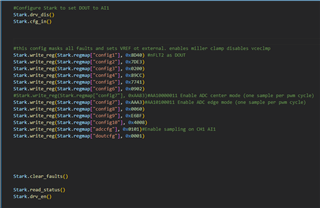
ADCDATA 1-8 registers return 0x0000 when read

Additional data:     
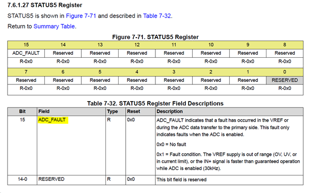
STATUS5 register indicates ADC fault (0x8000) 
STATUS4 register, bit 10 indicates nFLT1 fault on secondary side of gate driver (0x0400)
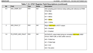
  • attempting to use the ADC1 register to read voltage divider data with a NTC thermistor to determine gate temperatures. 

The documentation says there are 3 possible sources of error, see below. I'm using the internal vref and I can measure it as 4.0 volts on the Vref output pin. Any suggestions as to how I might check the other two error conditions? 

  • Hi Tom,

    Thanks for reaching out. Can you please make sure that you have Vref is internal (0x1) in CFG8[bit4] if it's not supplied externally?

    Best,

    Pratik

  • Thanks for the reply Pratik! I just saw this after updating my original post above - yes, I'm using the internal Vref and I can measure it at the Vref output pin.

  • Hi Tom,

    Can you please try writing CONTROL2[bit15] = 0x1 to clear the fault and then read ADC data.

    If that still doesn't work, can you please provide the switching frequency and all the register maps along with chosen values. ADC_FAULT also happens for the below reasons.

    Best,

    Pratik

  • Hi Pratik - I'm thrilled with your timely responses - thank you!  I'll have to modify my Simulink model to do debug writes.. I'll get back to you has soon as I have the result of the test... an hour or so. 

  • Hi Pratik,

    I did the write test;  wrote the CRC_DIS bit in CFG8 to 1, followed by writing Control2 bit 15 to 1 (it immediately clears) but it doesn't appear to effect the problem. I still get 0x0000 outputs from the ADCs when reading. I'll follow up with a dump of the configuration registers...

    Best,

    Tom

  • One additional note:  I have a red led on my board that flashes on assertion of nFLT1 from the gate driver(s). When I do the error clear write sequence described above, it does clear the error on nFLT (the ADC fault), but I'm still reading zeros from the ADC's.  If they were working, wouldn't I expect to at least see a couple of LSB's of bit toggle from noise in the ADC measurements? 

  • Hi Tom,

    You're right about the ADC FAULT which was due to power up. We think something in the probably missing in CFG. Can you please send the INPUT signal switching frequency along with every register needed for ADC configuration which would help us understand the situation better. We'll try our best to find the root cause of this issue.

    Best,

    Pratik

  • Morning Pratik!

    I believe we're switching at 20khz - but having just said that I think my model is not set up properly. Let me double check this and get back to you asap. I'm travelling today, so I might need to validate this tomorrow. 

    Here are the config register settings that we change, the others are set to the defaults. Note also that the order listed is the order we set the registers in. Could there possibly be an "order of operations" issue when we initializing the registers? 

    ADCCFG 0x0101

    CFG2 0x0A01

    CFG4 0x091C

    CFG7 0xAA94

    CFG8 0x0020

    CFG9 0x8F00

    Thank you again for all the help!

    Tom

  • Hi Tom,

    Thanks for the quick reply with all CFG values. We've checked your configured settings, and they look fine. We have something similar, and it has worked for us, please see the below image with our settings:

    We don't think the order matter, but you can try with ADCCFG at end in the order you've provided.

    Couple of things to check would be:

    1. Make sure the device enters configuration state with CFG_IN command before writing the CFG and ADCCFG registers.

    2. PWM only counts if it is transmitted to the secondary side, so if ASC_PRI_EN is high and ASC_PRI_IN is low there will be no PWM to the ADC.

    Please check the above at your end. We would also try your setting values and get back to you before end of next week.

    Best,

    Pratik

  • Hey Pratik!  I went back and reviewed my test model and since it is a subset of the entire application (which is where I found I couldn't read the adc regs) I hadn't included the part of the model that does the gate switching. No switching edges, no ADC conversions. So, I'm good to go now. But it does beg the question:   

    Is there any way to start an ADC conversion without gate switching occurring? 

  • Hi Tom,

    Yes there is. 

    The ADC requires IN+ input PWM pulses to begin sampling.

    Secondary side ASC can be used if the output needs to remain LOW.

    • There’s 2 ways secondary side ASC can be achieved.

    1.Digital isolator to give control AI5(ASC_EN) and AI6(ASC) pins

    2.Enable AI5 internal current source using SPI (AI6 should be shorted to GND2)

    • Steps to achieve this:

    1.Program AI5 and AI6 for ASC and enable AI5 internal current source.

    • This is done in configuration 2 mode.

    2.Go from configuration 2 mode to active mode (Output will be held low by secondary side ASC)

    • When gate driver transitions to the active mode the internal current source will bias an external resistor to pull AI5 high(Secondary side ASC enabled). With AI6 shorted to GND2 the output safe state will be LOW

    3.With the output being kept low by secondary side ASC give the necessary IN+ input PWM pulses to initiate the ADC

    4.Disable AI5 current source

    • Before beginning operation, the gate driver must be taken back to configuration 2 mode to disable the current source (Disable secondary side ASC)

    5.Go back to active mode to begin gate driver operation.

    Hope this helps.

    Best,

    Pratik