This thread has been locked.

If you have a related question, please click the "Ask a related question" button in the top right corner. The newly created question will be automatically linked to this question.

UCC27517A-Q1: UCC27517A-Q1

Part Number: UCC27517A-Q1
Other Parts Discussed in Thread: UCC27517A, UCC28180, UCC25660

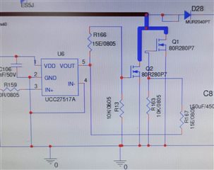
We are using gate driver ic UCC27517A-Q1  with our (pfc + llc) controller, our pfc controller output is 390v- 2.99a.

we are facing some problem, in gate driver ic lower mosfet(Rol) failed after some time and external mosfet short (32a-650v)  when we run circuit with full load .

its a ev charger and output dc is 65v -15a, input ac 170v to 270v. please suggest us solution.

1000w_1 pfc.pdfWSJM65R099DX Preliminary.pdf

  • Hi Aditya,

    Can you please reconfirm the VDD and IN voltage you are inputting into the UCC27517A? Can you also share waveforms of the input, output, and VDD voltage from before and after the failure?

    Thanks,
    Rubas

  • Dear sir,

    Please find the waveform of  GATE DRIVER IC IN pin, vdd pin, out pin ,mosfet drain pin before failure . one more thing  gate driver IC is suddenly failing .It's failing even after two hours or 2 days 

    this waveform taken on input 180VAC and output dc 54.50v-15A (with battary)

    IN PIN =GREEN WAVEFORM 

    VDD= YELLOW WAVEFORM

    VOUT= BLUE WAVEFORM 

    MOSFET DRAIN PIN = PINK WAVEFORM 

    Thank 

    Aditya arya 

    phn no -91+ 8077205198

  • Hi Aditya,

    Thanks for providing the waveforms. There looks to be significant noise on the VDD line, which may cause problems with the IN pin. I have a feeling that the IN pin gets shorted to VDD internally when the device fails, which causes OUT to be permanently high.

    Please confirm this on a failed device by measuring the resistance of the IN+ pin for two cases: with VDD and without VDD. On a good device, the resistance measured should be around 230kOhms, which is the internal pull-down resistance of the IN+ pin. On a bad device, it should either give a short or open measurement. Please let me know what the results are for when VDD is applied and for when VDD is not applied.

    Once this is confirmed to be the case, then I would recommend implementing an RC filter on the VDD line to reduce noise to a safe level. I would also make sure that the bypass capacitor is very close to the device. Please let me know once you confirmed the failure.

    Thanks,
    Rubas

  • Dear Rubas

    We have checked

    1. OK IC pull down resistance it is showing in Mega Ohm - 2.6MOhm , surprised showing 230K pull down in datasheet but multimeter is not showing. Even same for pull up not showing on IN- pin

    2. Faulty IC is also showing same as ok IC. but as i mentioned initially in faulty IC it is output sink mosfet shows short ( out to ground - short)

    3. while Vdd power up same condition as above.

    4. We have kept Vdd cap very close to IC- please check layout screenshot, but yes value is 100nf , we will increase cap value to 2.2uF.

    5. Our observation is when we are operating on Low input Vac then Gate drive IC get damaged

    Q1. Please suggest possible reason on the basis of above observations

    Q2. can you suggest if we have selected gate resistance value properly 15E for each mos and other components of gate driver ic related.

    Q3. We recalculated and using gate resistance 4.7E for each mosfet now , Vdd cap - 2.2uF and changed range of operation from 150- 265Vac and testing our board.

    Q4. Please suggest also  RC fillter  for VDD 

    Pease find the layout screen short


  • Hi Aditya,

    1. On a good IC, measuring IN+ to GND will give 230k, and measuring VDD to IN+ will show open. Since you're measuring 2.6MOhms on IN+, which is basically open, please double check if you are measuring with the correct reference. This should be the opposite for measuring IN- resistance, where measuring IN- to GND will show open, and measuring VDD to IN- will show 200k.

    I'm curious to know how you measured the pulldown MOSFET, in which you got a short. If you measured a short, then there would not be any output. To test to see if the pulldown NMOS in the output stage is good, then measure from OUT to GND with a multimeter on the diode setting. A good NMOS will measure around 0.5V, while a bad MOSFET will be either close to 0V (shorted), or it would measure open, which could potentially be your case of OUT being permanently high.

    If both the input and output stage are tested to be good, then it could potentially be something in the internal circuitry of the device that may have gotten damaged, which would most likely be caused by VDD noise.

    2. Gate resistances are used to control the rise/fall time of the output. There is no "correct" value, as it's up to the designer on how much they want to control the rise/fall time. However, higher gate resistance could potentially reduce transient spikes as the output switches. Please refer to this guide in selecting gate resistors: https://www.ti.com/lit/ab/slla385a/slla385a.pdf

    3. A higher bypass capacitance is better, but also do consider the potential parasitics when your bypass cap is too high. Your capacitor placement in the layout looks okay to me as well. Your input VAC shouldn't be the reason for failure, but I'm curious to know if you have data on what the typical VAC is when the driver IC starts getting damaged. If your input VAC is high, the driver IC remains good, correct?

    4. You need to measure the frequency of your noise to accurately calculate an RC filter. Realistically, even 1ohm resistor would drastically reduce the ringing. You also want to be careful in not using a high resistor value as it would create unnecessary voltage drop.

    Please let me know if the tests I mentioned helps your case, and if the increase in bypass capacitance helps as well. If there's any data about the relation between input VAC and device IC failure, please let me know about that as well.

    Thanks,
    Rubas

  • Dear Rubas 

    1. a. IN+ to GND showing open in both faulty and OK IC. IN- to Vdd showing 180 K in both faulty and ok IC.

        b. when i placed on IC on bare board and power up 15V (vcc to gnd ) checked  IN+ to GND is 400K in ok IC 420K in faulty IC and for IN- to GND results are approx 180K 

    I am sure 230K mentioned as pull down and we are not able to measure without power up , IN+ must be having some internal ck inside before this pull down resistor.

    We ensure our measurement/ reference is with standard equipment and carefully we are doing.

    in faulty IC we checked out pin to gnd is short , in ok IC we checked it gives diode Vf.

    2. New value 4.7E we selected and finding its not over damp or overshoot in start and quick pull down in end of on time.

    thanks will refer to your shared note too.

    3. though we are unable to simulate the field condition , but in multiple board testing in 2 boards we found on lower Vac switch on our gate drive ic failed.

    so we decided to shift brown in to 150Vac , gate drive cap 2.2uF as datasheet also refer for higher gate drive current and changed driver resistance to 4.7E. testing this change in 5 boards not showing failure.

    4. dint find impact of 1E sharing below waveform.

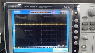
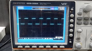
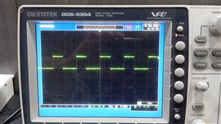
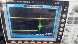
         <----- with 0 ohm vdd

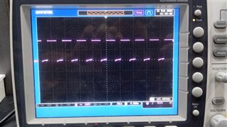
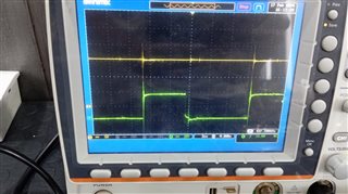
      <-------- with 1 ohm vdd

    seems no impact when we add 1 ohm register at vdd pin.

    Thanx

  • Hi Aditya,

    Our expert is currently Out of Office as we're observing Mon (2/19) as a US holiday. We'll get back to you by the end of next business day.

    Best,

    Pratik

  • Hi Aditya,

    Thank you for your patience and apologies for the delay.

    1. Thank you for letting me know about this behavior. I will conduct some tests and research to see if there are any more additional criteria to consider when measuring resistances for this device.

    For the diode test on the output, it is interesting how you are measuring a short, because then there would be no output at all. Before I consult the IC design team, I would like to confirm what the actual failure behavior is? When the IC fails, is the OUT signal high, or is there no signal at all?

    2. Glad to hear it, hopefully that guide I sent helped.

    3. Just to confirm, when you increased the VDD bypass capacitance and reduced the gate resistance, the failures stopped? It would definitely be the case that the higher bypass capacitor would reduce noise and reduce the chances of failures.

    4. From the looks of it, it may be that the input pin also needs an RC filter. Similarly, I would recommend a smaller resistor value to avoid too much loss on the signal. You can also try to increase the resistor value on VDD (and input as well) and see if that helps, but be wary to not do it too much to create voltage drop. I would also try to figure out what the noise frequency is. From your most recent waveform, it does look like at least 25MHz, but it's probably higher. Here is a link to a simple RC filter calculator that you can use: https://www.digikey.com/en/resources/conversion-calculators/conversion-calculator-low-pass-and-high-pass-filter

    Thanks,
    Rubas

  • Hi Aditya,

    Along with my previous reply, I also want to reconfirm if the external power MOSFETs Q1 and Q2 are failing by short as well? If they are failing, then it is most likely a short failure from drain to gate, which ends up shorting the pulldown NMOS in the output stage of the driver. Is this failure a one time thing, or is it happening to every board that is built?

    Thanks,
    Rubas

  • Dear rubas,
    In our board, the gate driver IC is only failing, the mosfet is fine, we have found that the gate driver IC in our board has 20% rejection

  • Hi Aditya,

    Thanks for confirming that the MOSFETs are not failing and that the failure rate is 20% among the boards that were built. I'm not sure if you saw my previous reply, but I did have other questions that I was hoping to receive clarity on. I can ask them in this reply for your convenience:

    1. For the diode test on the output of the gate driver, it is interesting how you are measuring a short, because then there would be no output at all. I would like to confirm what the actual failure behavior is? When the IC fails, is the OUT signal high, or is there no signal at all?

    2. Can you also measure between VDD and OUT with the diode setting on multimeter and let me know what you observe on both failed IC and good IC?

    3. Even though it's most likely a failure at the output, I'm wondering that when you increased the VDD bypass capacitance to 2.2uF, the failures stopped? Was this increase in capacitance tested on new ICs, or did you also test it on the failed ICs?

    4. From the looks of it, it may be that the input pin also needs an RC filter. Similarly, I would recommend a smaller resistor value (10-100Ohms) to avoid too much loss on the signal. I would also try to figure out what the noise frequency is. From your most recent waveform, it does look like it is in the high megahertz, but it's unclear as it's not zoomed in. Here is a link to a simple RC filter calculator that you can use: https://www.digikey.com/en/resources/conversion-calculators/conversion-calculator-low-pass-and-high-pass-filter

    Thanks,
    Rubas

  • Dear rubas,

    Thanks for your support, we will now try to add RC filter on +IN pin and VDD pin in the next rev PCB.

    In failure IC we just check the reverse diode, OUT pin to GND pin shows continuity (shorting), no voltage, while in good IC it shows .520V. so that as per the block diagram you can see the following MOSFET failure.

    one more thing can you provide us reference design and UCC28180 and UCC25660 design tool for 1.2kw. (LLC )only and 2.2kw  (PFC+LLC).

    Application :- EV charger 1200watt
    Ac input :- 170v-265v
    DC output :- 60,72& 84v-20A,17&15A
    Application :- EV charger 2200watt
    Ac input :- 170v-265v
    DC output :- 60,72& 84v-37A,30&27A

    Thanx

  • Hi Aditya,

    Thanks for the response. Can you also run a diode test from VDD pin to OUT pin and OUT pin to VDD pin on a damaged IC and a good IC?

    I want to make sure that the pull-up stage is not damaged as well, as that could potentially open up more cases to examine. If only the pull-down MOSFET is shorted, then one possible reason for that case could be that the power device you are driving ends up getting damaged from something external, and current goes through the gate of the power device and back into the OUT pin of the gate driver. I have drew up a quick drawing to illustrate for when that case occurs, where blue is the current path:

    However, you did say in an earlier reply that the external MOSFETs are not damaged, so I am still curious to know if the pull-up stage is damaged or not.

    For the reference design and design tool, I would suggest making a new thread with those parts as my colleagues on the controllers team may provide better information. However, I have dug up an LLC design tool for UCC25660: https://www.ti.com/tool/UCC25600-DESIGN-CALC

    Thanks,
    Rubas

  • Dear Rubas,

    I am not talking about external mosfet  its not damage, i am talking about  gate driver ic internal mosfet (Rol) only 

  • Hi Aditya,

    I understand the case that the external MOSFET is not damaged, and it is the internal MOSFET that is damaged.

    However, I want to try to debug more in the case that there is more damage. Can you conduct a diode test from VDD to OUT and from OUT to VDD on a damaged IC? I would like to see if the internal R_OH and R_NMOS is also damaged.

    Thanks,
    Rubas