This thread has been locked.

If you have a related question, please click the "Ask a related question" button in the top right corner. The newly created question will be automatically linked to this question.

TLV61070A: Ground plane

Part Number: TLV61070A
Other Parts Discussed in Thread: LM5155

I am working on a design using the TLV61070.

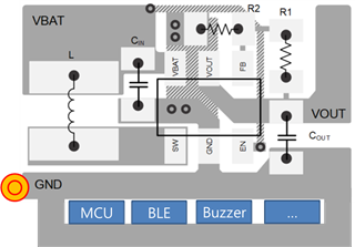
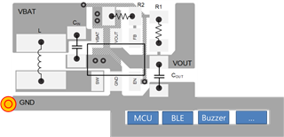
My PCB consists of the regulator, MCU, and amplifying circuit and the only sources of noise are buzzers and microphones.

In my PCB, most of signals are DC. There are a few AC signals, but they are low-frequency, below a few megahertz.

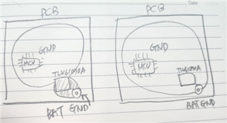
I have a question about how to handle the ground for the regulator.

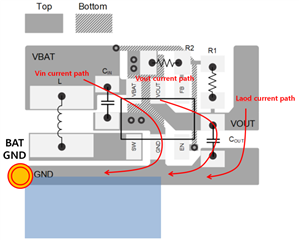
I have followed the guidelines to minimize the loop formed by SW-COUT-VOUT-GND and have designed the ground plane for the IC itself carefully.

However, I am unsure about whether it would be beneficial to connect the Battery ground (VIN GND) and VOUT GND together and create a ground mesh across the entire PCB.

Alternatively, it would be better to create a ground mesh across the entire PCB by only using the VOUT GND.

Could you please provide some guidance on this?

Regards JH Park

  • So, what I'm curious about is whether it would be better in terms of noise if the battery ground (VIN GND) is not directly connected to the MCU or other ICs. In other words, would it be preferable to establish a ground mesh with GND after passing through the regulator?

  • Hello Junghyun,

    There is no way to disconnect the input GND to the output GND on this device. You need to use the same GND level on the input side as on the output side.

    In general the device does not know anything about system grounding. So for the IC it self it is only interesting which signal you connect to the GND pin, but this is then the reference for all other signals on the IC (BTW, this is the case for most ICs).

    This means whatever you are doing on the system level, do not disconnect the input capacitor ground potential from the output capacitor ground potential on TLV61070A.

    Nevertheless, you can make sure to minimize noise to the system by properly layout of the power paths on the input side and on the output side. (in boost converter the output side is more important than the input side). Check out which path is taken by the high dI loops and make sure that these loops are closed by a solid ground connection.

    Best regards,
    Brigitte

  • The separation I was talking about was not about different levels, but about layout. 

    1. Merge all gnds of Vin and Vout to create the entire pcb gnd mesh. 

    2. The gnd of Vin is connected only to the gnd of vout, and the entire gnd mesh of the PCB is made using only the gnd of vout. 

       In other words, the battery gnd is not routed directly to the entire PCB including the MCU without going through the regulator. 

    Are there any pros and cons to each method?

  • Hello Junghyun,

    The pro of having one GND is that you have a very low impedance path and you are sure that none of the return paths that are created in the current loops are cut.

    The con is that you do not know exactly where the currents are flowing. Which could cause noise in areas where you do not expect it.

    If you are doing a proper layout of the loops, there should not be a big difference between the 2 solutions for this power level.

    If you are separating GNDs, you need to be very careful with the layout of the signals that are crossing the GND border. E.g. some supervising of the input voltage or so.

    Best regards,
    Brigitte

  • Hello Brigitte

    I think there was confusion in the conversation because I used the expression ground separation.

    What I mean is as shown in the picture below.

    The current path of Vin/Vout/Load will be as follows.

    What I'm curious about is the blue box area below. Shouldn't the ground in this area be directly connected to the load?

    What I am concerned about is the ground return path or ground current superposition, poor regulation, etc.

    My layout is as follow

    But, my boss told me that it is poor layout. He said the following layout is much better.

    But, I cannot agree why it is much better. And he gave the LM5155 EVM below as an example.

    In DC-DC, the GND paths for input and output should be layout as separately as possible.

    The cutting line in the red box below is also said to be used to isolate GND as much as possible.

    Is this really true? I really want to know.

    Regards Junghyun Park

  • Hello Junghyun,

    There is no definitive answer to your questions. Grounding is extremely dependent on the rest of the system behavior and therefore you will not find a definitive answer on which type of grounding is the best you can do. This is a question which is discussed even within the power community and the answer is in general: It depends.

    Best regards,
    Brigitte