Other Parts Discussed in Thread: TPS2065C, TPS25221, TPS2051C
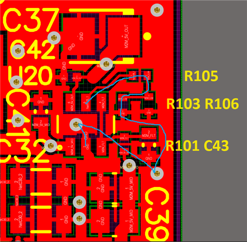
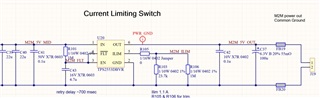
We are using a TPS2553 to limit current output from a DC/DC converter with 5 V output (not a USB application, though). The circuit is as shown below, set for a nominal limit of approximately 1.1 A with R103. R106 is not populated, as it was intended to allow trimming the current limit if necessary.
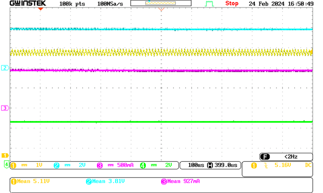
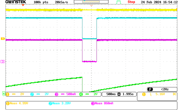
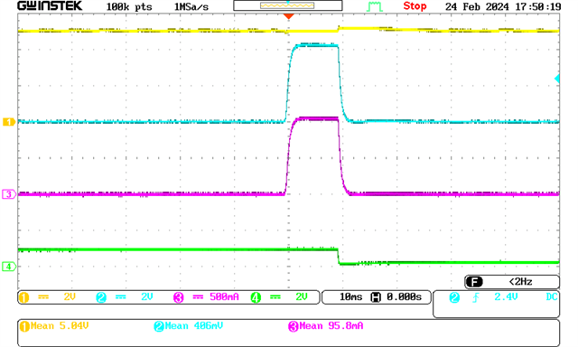
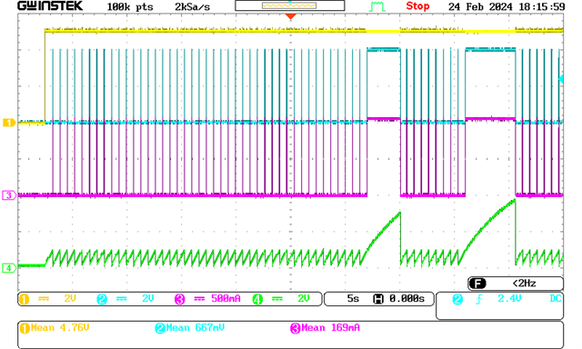
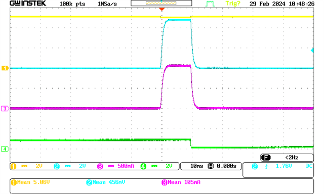
We are noticing differing behavior between boards in the batch of 75 that we built. As load is increased at the output, some boards hold the output at a fairly constant voltage until they reach the overcurrent limit, while some have a much greater amount of droop. Two examples are in the table below. These boards were loaded with a set of resistors, starting with approximately 4.9 ohms connected continuously, and then adding more resistance in parallel. We measured the output current and voltage with two DMMs, as well as viewing the voltage trace on an oscilloscope.
The table below shows the results for two boards as load is increased (not necessarily exactly the same in each row). The resistance values are calculated from Vout and Iout for reference, not from the parallel combinations of the various resistors used.
| SN59 | R103 = 23620 ohm | *** | SN53 | R103 = 23750 ohm | ||||
| Iout (A) | Vout (V) | Equiv.R | Comment | Iout (A) | Vout (V) | Equiv. R | Comment | |
| 0.953 | 4.63 | 4.86 | 0.967 | 4.73 | 4.89 | Note that this is already higher voltage than SN59. | ||
| 0.961 | 4.60 | 4.79 | 0.989 | 4.72 | 4.77 | |||
| 0.980 | 4.55 | 4.64 | 1.003 | 4.71 | 4.70 | |||
| 0.999 | 4.43 | 4.43 | 1.008 | 4.71 | 4.67 | 0.34 V higher than SN59 at similar current. | ||
| 1.006 | 4.37 | 4.34 | 1.062 | 4.69 | 4.42 | |||
| 1.010 | 4.28 | 4.24 | 1.099 | 4.64 | 4.22 | |||
| 1.012 | 4.21 | 4.16 | 1.103 | 4.56 | 4.13 | Current limit about 1.1 A. | ||
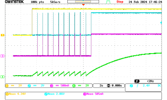
| 1.016 | 4.06 | 4.00 | cycling | Added 220 ohms more to above step, or ~20 mA additional if it weren't limiting/cycling. | ||||
| 0.978 | 3.76 | 3.84 | Current drops from previous row? | |||||
| 0.987 | 3.58 | 3.63 |
I measured the value of R103, in circuit at least (I know there are potential pitfalls, but I'm not ready to disturb the boards yet). The values are also in the table above, and based on the equations in the datasheet, I would expect the following range of current limits:
- SN53: 1.010 - 1.170 A
- SN59: 1.015 - 1.176 A, which is slightly higher than we would expect from SN53, but in fact it is quite a bit lower.
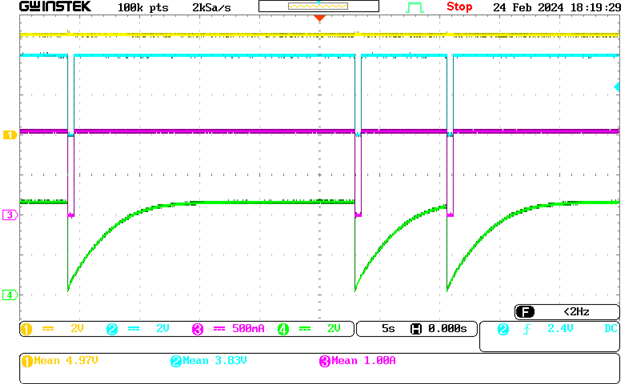
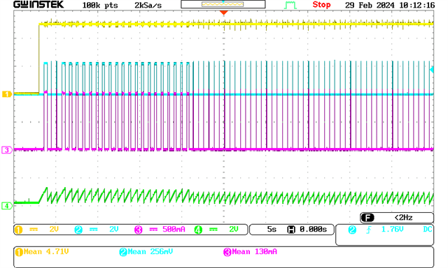
Any insight as to what could be happening here? From what I've been able to see and also measure with the DMM when the circuit is off, differences are minimal. Yet SN59 has a noticeably higher voltage drop and doesn't ever seem to go into shutdown. Furthermore, its current limit is right at the edge of what one might expect from the resistor value...that seems a bit unlikely. And as I increased load, the current limit decreased a little in the bottom two rows.
The shutdown behavior of SN53 is more common amongst the boards (though I tested them all with an electronic load for speed). It is also more like what I would expect from the "-1" version of the part (and in retrospect, the better behavior for this application). But this whole batch came off the same piece of cut tape, so it seems unlikely that there are mixed types here, and they likely even came from the same wafer.
I welcome your thoughts.
Kind regards,
Rod