This thread has been locked.

If you have a related question, please click the "Ask a related question" button in the top right corner. The newly created question will be automatically linked to this question.

USB-C-PD-DUO-EVM: USB-C-PD-DUO-EVM Configuration / Flashing problems

Part Number: USB-C-PD-DUO-EVM
Other Parts Discussed in Thread: TPS65987, TIDA-050012, TIDA-050014, TPS65987DDJ, TPS65987D, TPS65981, TPS65987DDK
Hello,
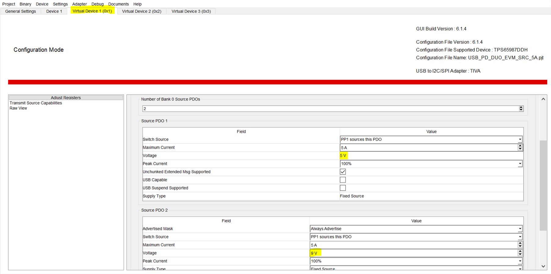
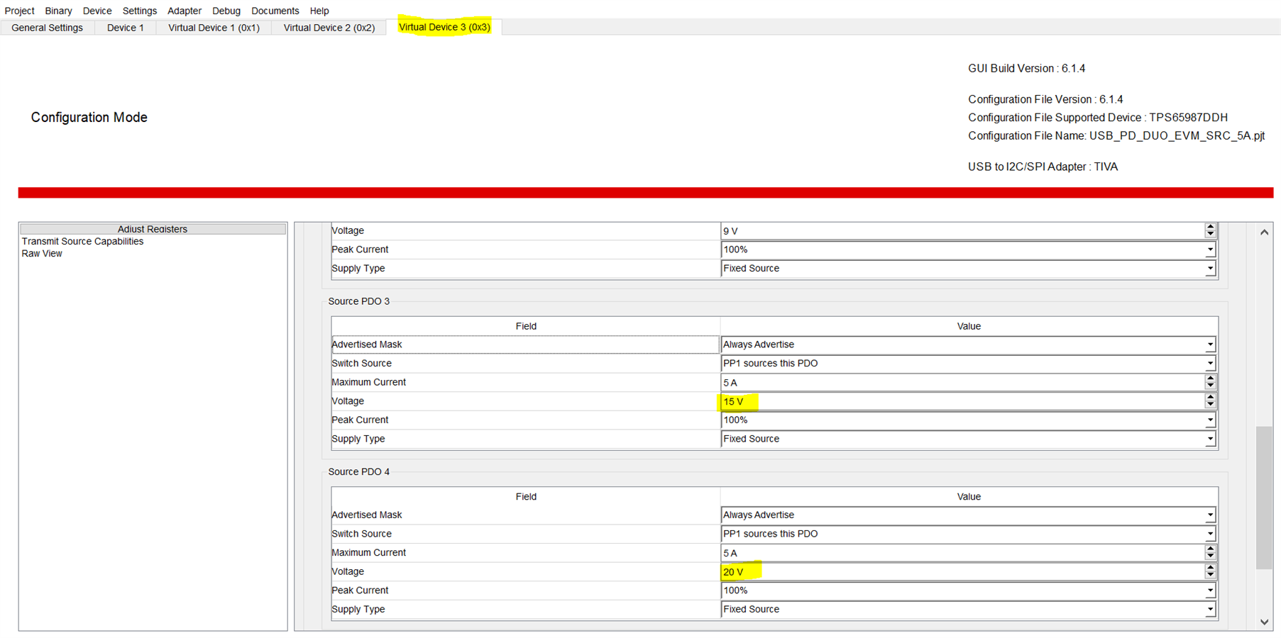
I'm trying to use the USB-C-PD-DUO-EVM by following the USB-C-PD-DUO-EVM User's Guide,
but I'm noticing that there are differences between the SW release date

"
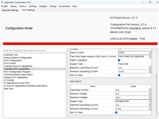
TPS65981_2_7_8 Application Customization Tool

GUI Version: 6.1.4

Release date: March 29, 2023
"
and the date of the manual
"SLVUBJ5–October 2018".
Q1 - Would it be possible to have a version of the manual aligned with the SW release date?

In any case I'm trying to take the first steps, but I'm having a lot of problems.

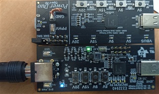
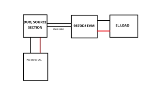
My HW is this: J1 powered with 19,5V, PC connected with a usb micro cable to the EVM.


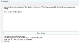
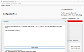
As for the interface connection, I believe this is there, in fact with the usb micro disconnected
I get this message 
"Exception Encountered during FTDI Adapter Selection:No FTDI I2C channels (I2C_GetNumChannels) detected, exiting....

<type 'exceptions.Exception'>

"
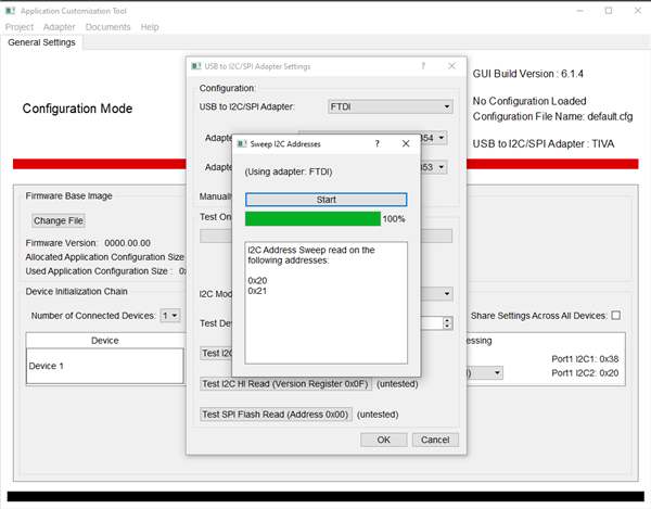
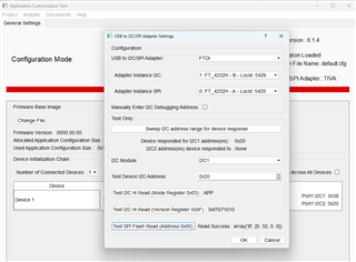
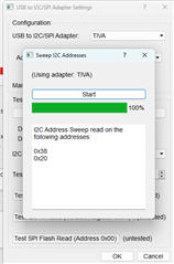
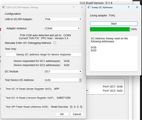
while when the micro usb cable is connected I get this popup when I click on "adapter"
 
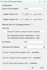
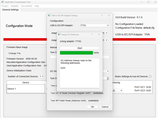
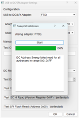
but if I perform the Sweep I2C Addresses it fails

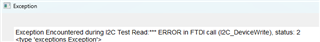
then if I try "TEST I2C HI READ (MODE REGISTER 0x03)

I get this FAIL MESSAGE

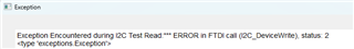
then if I try "TEST I2C HI READ (MODE REGISTER 0x0F)

I get this FAIL MESSAGE

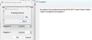
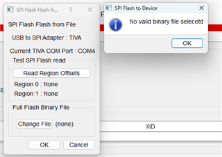
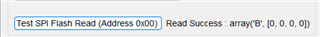
then if I try "TEST SPI FLASH READ (Address 0x00)

I get this SUCCESS MESSAGE

Q2 - how can I fix the problem (if any) with I2C?

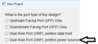
Q3 - which is the file to be loaded, that I cannot find source.bin or sink.bin?

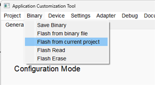
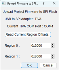
Q4 - when loaded a .bin file wuth "change file" button, which is the command to start flash?

Thanks

      Alessandro

  • I want to add some information about functional tests performed with the EVB

    Sink test

    EVB sink side connected with an USB TYPE-C to the PD power supply, Vout measured () on TP200 e TP201
    - 5V out mode with no load OK
    - 5V out mode @ 3A (4,6V) OK
    - 5V out mode > 3A switch off
    -
    - 9V out mode with no load OK
    - 9V out mode @ 3A (8,6V) OK
    - 9V out mode > 3A switch off
    -
    - 15V out mode with no load OK
    - 15V out mode @ 3A (14,4V) OK
    - 15V out mode > 3A swith off
    -
    - 20V out mode with no load OK
    - 20V out mode @ 5A (19,1V) OK
    -

    Note: current limitations is due to the PD_PSU limitations, in fact the PD_PSU expose the same behaviour with another sink board

    Source

    EVB source side connected with an USB TYPE-C to an external sink board, Vout measured () on D3/A - GND
    J1 supplied with 20V @ 6,5A limit
    - 5V out mode with no load OK
    - 5V out mode @ 5A (5,2V) OK
    -
    - 9V out mode with no load (9,4V) OK
    - 9V out mode @ 5A (9,4V) OK
    -
    - 15V out mode with no load (15,4V) OK
    - 15V out mode @ 5A (15,4V) OK
    -
    - 20V out mode with no load (20,0V) OK
    - 20V out mode @ 5A (19,1V) OK
    -

    Source + Sink

    EVB source side connected with an USB TYPE-C to the sink side, Vout measured () on TP200 e TP201
    J1 supplied with 20V @ 6,5A limit
    - 5V out mode with no load (5,2V) OK
    - 5V out mode @ 0,98A (5,0V) OK
    - 5V out mode @ 1A switch off
    -
    - 9V out mode with no load (9,4V) OK
    - 9V out mode @ 3A (9,0V) OK
    - 9V out mode @ 3,1A switch off
    -
    - 15V out mode with no load (15,4V) OK
    - 15V out mode @ 3A (15,0V) OK
    - 15V out mode @ 3,1A switch off
    -
    - 20V out mode with no load (20,0V) OK
    - 20V out @ 5A (18,5V vs 19,5V on PP_HV of the source section) OK

    Since the funcionality of the source section aloows 5A, it means that the sink section is programmed to limit at different currents. This means that is mandatory to program thresholds.

    Can you please confirm that?

     Thanks

    Alessandro

  • Hi Alessandro,

    1.) We do not have an updated version of the user manual for the 6.1.4 GUI. It is possible that the manual has been updated since then. The information should still be largely applicable regardless.

    2.) The issue is with the USB-PD-DUO EVM, the source and sink boards (top and bottom) are separate and do not share power. There are separate PDs on the boards. If you power the source board (top) with 19.5V barrel jack, the sink board (bottom) will not be powered. Since the FTDI chip is located on the sink board, the chip itself will be powered via micro-USB cable but the PD on the sink board will not be powered. This is why the sweep fails. Please power the sink board (bottom) via type-C port or jumping the SYS_PWR over from the source board.

    3.) The binary file used for the PD on the source and sink board are the same. It is the app config GUI settings that will change. Why do you wish to change the PD configurations on the board? We typically do not touch this at all since the USB-PD-DUO is designed to be a working out of package solution. Keep in mind if you change the source/sink PDO capabilities, the buttons on the board may not work properly. If you wish to test purely the TPS65987 PD controller, I recommend using a TPS65987EVM.

    4.) After loading a .bin "Firmware Base Image" file, you can use the "binary" tab at the top to "flash from current project".

    Best,

    Alex

  • Hi Alex, thank you for information useful to flash, I will try it asap.

    About the need to change setup it is due to behaviour of the sink section that has different current support for different working voltages, l reported the measures in my further comment two days ago "I want to add some information about .... ", then the goal is to set the sink section to allow 5A at all voltages.

    Please let me know if I performed the measures in a wrong way.

    Thanks

         Alessandro

  • Hi Alessandro,

    It is ok to change the source/sink capabilities on the PD DUO EVM. However, keep in mind that the PD on the EVM does not do current limiting or OCP function as a sink. PD will only do current limiting at 5V as a source, and OCP at >5V as a source. The current limiting and OCP functions are performed by the source side PD controller. Changes to the sink side PDOs are still needed to ensure the proper PD contract is negotiated, which the far-end source will use to decide its OCP threshold.

    Best,

    Alex

  • Hi Alex,
    sorry but I can't understand: I performed two types of tests which I describe below. One test involves the source section of the EVB and the sink section of the EVB. In these conditions I can obtain no more than 1A with Vbus at 5V; no more than 3A with Vbus 9V; no more than 3A with Vbus 15V; 5A with Vbus 20V. Another test involves the source section of the EVB and an external sink board. In these conditions I can obtain 5A at all voltages. This made me deduce that the difference between the two situations was the sink card sending different requests to the source card. If it were up to the source part refusing to go beyond a certain current, it would reject it in all situations, I don't get it.

    Thanks
    Alessandro
  • Hi Alessandro,

    The behavior you see when connecting the source side of the board to the sink side of the board is due to the PD source capabilities and PD sink capabilities of each board. I agree with you on the reason behind the different behavior. The sink side is probably requesting a lower current contract than the max the source can provide. Have you been able to successfully change the configuration of either the source or sink board?

    Do you have a PD analyzer tool (totalphase, ez-pd)? If not, I can test it using mine and let you know definitively what contract is being advertised and requested when the source board is connected to the sink board on the PD-DUO-EVM.

    Best,

    Alex

  • Hi Alex.
    I am not yet in a position to change the configuration for two reasons: I do not have a tool that allows me to create the content to write to the CHIP, and I have not yet been able to communicate with the CHIP itself.
    I tried to access the EVB again to try to test the interfaces after your suggestion to power the sink section correctly. The sink section is certainly powered as the Vbus LED is on, the 5V LED is on and there is a voltage of 5.2V on the TP200 and TP201 test points.
    I ran the "sweep I2C Addresses" test and it fails; I ran the "TEST I2C HI Read (mode register 0x03)" test and it fails; I ran the "TEST I2C HI Read (mode register 0x0F)" test and it fails; I ran the test "TEST SPI Flash Read ( Address 0x00) and it says "Read Success: array ('B',[0,0,0,0])". These checks were carried out both with the jumper in the SINK position and with the jumper in the SOURCE position.
    I don't have a Power Delivery analyzer, the "total phase" model may no longer be available (www.totalphase.com/.../).
    This may be a good substitute for "EZ-PDTm Protocol Analyzer". I will try to get it purchased, in the meantime please let me have the data, if you can measure it, thanks.

    Thanks

    Alessandro

  • Hi Alessandro,

    When I connect to the FTDI chip on the USB-PD-DUO-EVM and try sweeping for I2C address responses, I see this result:

    This is what you should expect to see. I have powered the source side board with barrel jack supply and connected the sink side with the source side via type-C cable, so both are powered. When you see the sweep fail, are you seeing a no address response result or is the green progress bar not moving? Both could indicate a bad FTDI chip or connection on the board.

    For the Source to Sink board connection, I have verified on my board that the USB-PD-DUO-EVM sink board is indeed configured to only request 5V 0.90A, 9V 3A, 15V 3A, and 20V 3A. The source side board has the following source PDOs configured: 5V, 9V, 15V, 20V all at 3A max. It is interesting that you were able to pull 5A using an external sink board connected to the PD-DUO-EVM, as this should not be allowed. 

    Source PDOs advertised by PD-DUO-EVM:

    Questions for you:

    1.) What is the far-end external sink board you are using? Is that programmed to request 5A? If it is, the PD-DUO-EVM should accept the request but set current to 3A max.

    2.) How are you loading and drawing 5A current with the external sink side connected? 

    3.) You can adjust the sink side PD sink PDOs to 5A on the PD-DUO-EVM, however, the source side must be adjusted to advertise 5A max source PDOs as well. For all TI PD controllers, we do not do any OCP or current limiting in the sink power role. This is up to the source side. 

    4.) Please collect PD logs of your connection between PD-DUO-EVM source board and external sink board once you have the proper tools, I am interested in seeing what the contract negotiated was that allowed 5A. 

    My PD logs of source to sink connection. Please use TotalPhase Data Center software to view.

    PD_DUO_EVM_Source_To_Sink_5V_9V_15V_20V.tdc

    Best,

    Alex

  • Hi Alex

    "When you see the sweep fail, are you seeing a no address response result or is the green progress bar not moving? Both could indicate a bad FTDI chip or connection on the board."

    I see the bar moving, but at the end there is the fail message. Boards are supplied both (please, see previous message). Please provide me a method to diagnose this.

    About the current limit operation, I repeated the test with almost the same results, but with the analyzer used to lo data. (I have a Cypress not a TotalPhase).

    testToday.zip

    Please let me know how estabilish if the source board is configured to provide 5A in any condiction an how to test it with TI sink board.

       Thanks

    Alessandro

  • Hi Alessandro,

    As we can see from the PD logs you collected and the logs I have seen on my side, the negotiated PD contracts when any sink device is connected to the USB-PD-DUO-EVM source board are 3A max for 5,9,15,20V. The TPS65987 on the source side of the PD-DUO-EBM should be shutting off the power path once the current draw from the far-end exceeds 3A. You can see this happen correctly in the 5V, 9V, and 15V contracts with PD-DUO-EVM source and sink sides connected. If the current draw from the sink is allowed to exceed 3A for the 5V, 9V, 15V, or 20V contracts, then OCP is not working properly in the TPS65987 on the source side board. I will have to test the OCP on my end to verify reproducibility.

    The way you are testing the OCP function with PD-DUO-EVM source and sink side connected is correct. I do have a question about the test setup with the external sink board. What do you mean by "Vout measured () on D3/A - GND"? Where is this measure point located? I am assuming this is also where you have the load hooked up to draw current.

    Best,

    Alex

  • Hi Alex,

    "The way you are testing the OCP function with PD-DUO-EVM source and sink side connected is correct. I do have a question about the test setup with the external sink board. What do you mean by "Vout measured () on D3/A - GND"? Where is this measure point located? I am assuming this is also where you have the load hooked up to draw current."

    Yes I measured the output on the sink board that exposes two test points, and I draw current from there with an electronic load in CC mode

    Thanks

         Alessandro

  • Hi Alessandro, 

    I am assuming you are doing something similar for the external sink board as well (not the PD-DUO sink board). 

    I aim to test this out tomorrow and will let you know what results I see for OCP/current limiting on the PD-DUO-EVM source board.

    Best,

    Alex

  • Hi Alessandro,

    I was able to test OCP with my USB-PD-DUO-EVM today. My PD-DUO-EVM has the default FW that the board comes with out of the box.

    I was able to see similar OCP issues as you do with the source side connected to the sink side. The 9V, 15V, and 20V contracts all allowed me to draw 5A of current while loaded before shutting off. However, I was able to fix this OCP issue by re-flashing the source and sink side of the USB-PD-DUO-EVM with the latest FW and project configuration from the 6.1.4 GUI. I believe there was an OCP issue in older FW that the EVM is pre-flashed with on fabrication, that was fixed in newer FW available in the GUI. Please follow the below steps to re-flash the board:

    1.) Open the 6.1.4 GUI

    2.) Go to the project tab (upper left) and select new project.

    3.) Select TPS65987DDH, then select TIDA-050012 Source Board. This is the project configuration for the PD-DUO-EVM source side PD.

    4a.) When flashing the source side, power the source side of the EVM with barrel jack supply. Jump the middle pin of J202 with the SRC pin (SRC SNK jumper).

    4b.) When flashing the sink side, power the source side of the EVM with barrel jack supply. Jump the middle pin of J202 with the SNK pin (SRC SNK jumper). Connect the source and sink side of the EVM using type-C cable.

    5.) Ensure the FW Base Image is set to TPS65987_88_F707_10_10.bin.

    6.) Perform an adapter sweep for I2C response over FTDI. This must be successful to continue.

    7.) Flash the PD using the binary tab (upper left) - flash from current project.

    8.) Repeat steps 3-7 with the TIDA-050014 Sink Board project for the sink side.

    By following the above steps, you should be able to reprogram the EVM with the latest FW that includes the OCP fix.

    If you still cannot get any address response over I2C when doing the FTDI adapter sweep, please swap to a different micro-USB cable or reinstall the GUI tool. I was also having trouble with the adapter sweep but resolved this when using a different micro-USB cable.

    Best,

    Alex

  • Hi Alex,
    the good news is that I managed to do the FW upgrade following the instructions, and actually the communication problem seemed to be linked to the connection, even if that cable works with other devices, but still OK.
    Before doing the update I noticed another problem: the EVB didn't start, it was necessary to turn it off and restart it several times. Now it seems more stable.
    The values ​​that I now measure are these
    5V ---> max 1.4A
    9V ---> max 3.8A
    15V ---> max 3.8A
    20V ---> max 3.3A
    using the TI sink board.
    This is all good as far as upgradeability goes, but we would need to configure the EVB differently if that were possible. We are not interested in the OCP function on board, we manage it externally, we would like to set 5A to all operating voltages. Can it be configured this way?

    Thanks

        Alessandro

  • Hi Alessandro,

    Yes you can change each source PDO in TX Source Capabilities register (0x32) of the source side PD to 5A max current. You'll notice in the GUI project there are 4 tabs up top, Device 1, Virtual Device 1, Virtual Device 2, Virtual Device 3. You will need to change the source capabilities in each of these configurations. If you want the sink side PD-DUO board to request 5A contracts, you will need to make similar changes to the sink capabilities on the sink side PD. Then follow the same instructions I sent before to re-flash the PD-DUO board.

    I have made the changes to these projects and attached them here. But the above would be how you change the current capability in the project configurations for 5A. Please follow the same instructions I gave before to re-flash the PD-DUO source and sink boards.

    USB_PD_DUO_EVM_SRC_5A.pjt

    USB_PD_DUO_EVM_SNK_5A.pjt

    Best,

    Alex

  • Hi Alex, 

    I tried to change settings, but while I can find the 5V settings, it is not clear where to change the other voltages settings

    Thanks

       Alessandro

  • Hi Alessandro,

    You can change the max current for the 9V, 15V, and 20V source PDOs in virtual device 1, 2, and 3 respectively. Make sure to change every PDO in every device/virtual device. Each time you press a voltage level button on the source side of the PD-DUO-EVM, the EVM will load a different configuration with a different set of source PDOs. This is for the purposes of the PD-DUO-EVM only, in your system you will only need to have one device configuration with multiple source PDOs.

    In the two source and sink projects I sent two messages ago, I have already changed the max current to 5A for all source and sink PDOs.

    Best,

    Alex

  • Hi Alex,

    I flashed the two project you sent me. I tried again to load the sink board (TI Sink board and External sink board).

    With TI sink board

    5v - max 1,5A

    9,15,20V - max 3,5A

    With External sink board1

    5v - max 3,5A

    9,15,20V - max 3,8A 3,5A not allowed (skip ango directely to 5V when try to go to 20V)

    With External sink board2

    5v - max 3,5A

    9,15,20V - max 3,8A 3,5A 3,5A

    It seems to me that the current limit setting is not met.

    Furthermore, please esplain me once more hw to set it, because I continue to see only 5V in the gui in the differet tabs.

    Thanks

       Alessandro

  • Hi Alessandro,

    Were you able to acquire a PD analyzer. We need to see the PD messaging to know what was offered and requested during negotiations. If the max current will not go above ~3A, then this means 3A max was still negotiated by the PD connection.

    If not, I can load the configurations onto my board and collect the logs.

    To see the 9V, 15V, and 20V PDOs, you need to go to virtual device 1, 2, and 3. See below:

    Note that the "Number of Bank 0 Source PDOs" field at the top will dictate how many source PDOs are present in the configuration.

    Best,

    Alex

  • Hi Alex,

    I some measure this morning. In attach you can find all.

    Setup.txt
    Setup
    I Flashed again the two project USB_PD_DUO_EVM_SNK_5A.pjt on the sink side 
    and the USB_PD_DUO_EVM_SRC_5A.pjt on the source side.
    
    About connections, TI source and TI sink connected with analyzer between the two sections.
    
    Power out measures
    5V with load CC rising from 0A to 1,5A, from start to line 455 are lines generated to the analyzer when the current limitation occours, followed by other connection attempts.
    
    Next lines to 541 line there are:
    - press 9V key on the source
    - press 9V key on the source
    - rising load current until about 4A ---> limitation
    Next lines to 627 line there are:
    - press 15V key on the source
    - press 15V key on the source
    - rising load current until about 3,6A ---> limitation
    Next lines to 714 line there are:
    - press 20V key on the source
    - press 20V key on the source
    - rising load current until about 3,4A ---> limitation
    
    
    2024 21 03 setup - measure.csv

    Thanks

      Alessandro

  • .... I nticed that the current reading is a very unstable value from what the analyzer can read. The below image reports a 400ma LOAD over a 5V out setting, the external current is veri stable, but the board seams to read this

    Maybe that some filter is necessary for this measure, I mean numerical filter, is it possible?

    Thanks

        Alessandro

  • Hi Alessandro,

    Could you share the PD log file in the non-CSV form? The CSV form does not decode the PD messages, so I cannot see max current being advertised and negotiated. Depending on what PD analyzer you are using, the file extension for the logs will be different. For example, EZ-PD analyzer would produce a .ccgx3 file that can be opened and decoded by the software tool.

    Best,

    Alex

  • Hi Alex,

    I was getting ready to take the measurement and send you the trace of the analyzer in the desired format, but I'm having 
    problems with the DUO EVB. I can flash as many times as I want, and it always works. The problem is that it no longer starts:
    the source section does not generate the 5V vbus. However, if I keep the battery off for a long time and then turn it back on
    it seems to start again. If I turn off it and turn it on again, it won't start. It had already happened to me in recent days.
    It seems as if something must be discharged that prevents a correct restart. Any suggestions?

    What can you tell me about the current reading seeming very noisy? Perhaps it is necessary to act on the parameter that allows pulses of a higher percentage

    to be tolerated (for example by setting 200%, which is usually used by control chips as a circuit breaker).

    Thanks 

         Alessandro

  • ...... 

    When I say "I can flash as many times as I want", I'm referring to the SRC section obviously, because without VBUS I can't 
    flash the SNK section...

    Alessandro
  • Hi Alex,

    I have another question about this device/EVM:

    If we need to implement a dual role application using this EVB, what kind of action are necessary? Can you please sugget this action over the existing schematic (with rapid notes)?

    Waiting for updates from you, thanks

    Thanks

       Alessandro

  • Hi Alessandro,

    Sorry for the delayed response.

    The current reading looks odd to me as well, I haven't seen it that inconsistent before. Can you confirm the current reading using other methods? Current measurements from PD analyzer tools are not the most accurate. I'm not sure what could cause that but I would need to check with my team.

    The PD-DUO EVM is designed and configured to only support single power roles on either side. This is the reason it comes in a pair. To have a single PD configured with both source and sink power role capabilities at the same time, I would recommend ordering the TPS65987 EVM on ti.com. You can use the TPS65987DJ EVM to achieve this application.

    There may be a way to use the sink side board in a dual role power configuration, if you are able to hook up your power supply to the PPHV test point and make sure you disconnect the power supply from the board before you swap to a sink role. You would need to change the configuration project to enable the power paths as source and sink, as well as add source PDOs. I don't see hardware support for sinking power on the source side board, so I would not recommend that.

    Best,

    Alex

  • Hi Alex,

    1 - about current reading I confirm that with an external amperometer the value is very stable

    2 - thanks for the tip to use the alternative board for the dual role

    3 - what is very important now, is to solve the false start issue like I wrote in last comments :

    "I was getting ready to take the measurement and send you the trace of the analyzer in the desired format, but I'm having
    problems with the DUO EVB. I can flash as many times as I want, and it always works. The problem is that it no longer starts:
    the source section does not generate the 5V vbus. However, if I keep the battery off for a long time and then turn it back on
    it seems to start again. If I turn off it and turn it on again, it won't start. It had already happened to me in recent days.
    It seems as if something must be discharged that prevents a correct restart. Any suggestions?"

    Thanks

         Alessandro

  • Hi Alex,

    I was studying the TPS65987DJ Evaluation Module manual. I have some questions to ask about this. In the manual it says that the EVM behaves like the port of a notebook, so it will certainly be ready to manage both use cases as a sink and or a source through the use of the TIVA controller. What I don't understand is:

    - How do I select the working voltage in the case of use as a sink, i.e. if I decide to ask for 15V 5A, what do I do?

    - The 20V power supply on J9 must always be active, so what happens if the sink function is active which would therefore bring a 5,9,15,20V voltage of your choice always diverted to J9?

    Thanks

          Alessandro

  • Hi Alessandro,

    When the PD-DUO-EVM source side is not providing 5V at start, do you see any PD contract being negotiated after the connection? What happens if you press the 5V, 9V, ... buttons on the source side board?

    My responses to your questions:

    1. How do I select the working voltage in the case of use as a sink, i.e. if I decide to ask for 15V 5A, what do I do?
      1. If you are using TPS65987DDJ as a power sink, the far-end PD acting as the power source would send its source capabilities in the form of a PD message over the CC lines after connection. This is the far-end source advertising its capabilities, from which the TPS65987DDJ would request a certain advertised PDO through another PD message. The far-end should accept the request, and then follow that with PS_RDY to signify that it is ready to source power. All of this is done through PD messaging. Using a PD analyzer, you would see this happening. 
      2. If the far-end source does not send its source capabilities on initial connection, the TPS65987DDJ would send a hard reset to reset the connection and attempt to get the other side to advertise capabilities. The source always starts the PD negotiation process on initial connection.
      3. If after initial connection and PD negotiation, you want the TPS65987DDJ to change the negotiated PDO, you would send a Get Source Capabilities "GSrC" command to the PD (over I2C) to have it request source capabilities from the far-end PD.
    2. The 20V power supply on J9 must always be active, so what happens if the sink function is active which would therefore bring a 5,9,15,20V voltage of your choice always diverted to J9?
      1. Yes, on our TPS65987DDJ EVMs, the sink path is connected to SYS_PWR on the system side, which is connected to the barrel jack at J9. We rely on RCP protection to keep this in safe boundaries. If you want, you can remove the jumper connecting the PP_HV1 sink path to SYS_PWR at J4. This will allow the system side of the sink path to float instead. If you do this, then barrel jack power must be present at J9 to power the board.

    Best,

    Alex

  • Hi Alex,

    sorry for the amount of questions.

    "When the PD-DUO-EVM source side is not providing 5V at start, do you see any PD contract being negotiated after the connection? What happens if you press the 5V, 9V, ... buttons on the source side board?"

    For the 'DUO The real problem here is that it is not a fixed replicable problem. The "false start" appens not always, but sometimes. The last time I tried to show it to my colleague, it never appened, so if I try to measure any PD contract being negotiated after the connection to find somethig wrong maybe a difficult work. It would be very useful to have someting to check without disconnecting anything, I will try some more verifications.

    For the TPS65987DDJ it is clear your reply, thanks.

    Thanks

           Alessandro

  • Hi Alessandro,

    I have not seen the false start issue on the PD-DUO board but the best way to debug or diagnose this would be to collect PD logs with your PD analyzer tool when connecting to the PD-DUO source board. You can always have the PD analyzer connected and capturing during tests. Additionally, if you can gain access to and probe the CC pins, VBUS pin, and PPHV pin using resistors or test points, this would help as well.

    When the PD-DUO-EVM source side does not provide 5V at the start, then this means either a type-C connection on the CC pins was not made, or that the PD controller on the EVM is not turning on its power path. Measuring the CC pins (analog capture) will help see if a connection was made and measuring the PPHV and VBUS pins would help see whether the power path was enabled during the failure. All of this can also be seen by using the debug mode in the GUI via the micro-usb port, if you can establish a reliable connection.

    Best,

    Alex

  • Hi Alex,

    this morning Itried again to start the DUO Board, it doesen't start the Vbus again. I read some information over it to provide to you:

    Board supplied with a 20Vin

    • D2 and D3 are lit
    • on Tp3 I measure 3.3V
    • on R22 I measure 20V
    • on R23 I measure 5,2V
    • on ***C21 I measure 0V
    • on C22  I measure 1,8V
    • on C23  I measure 3,3V
    • on C24  I measure 5,2V
    • on C25  I measure 5,2V
    • C26  I measure 3,3V

    This is what I see

    Connecting the usb micro cable to the board the interface works fine

    Connecting the analyzer there is no event registered.

    Any Idea? Can be investigated someway?

    Thanks

         Alessandro

  • Hi Alessandro,

    Is this test done with PD-DUO-EVM source side connected to sink side? Or was it done with a different sink board?

    C21 capacitor is connected to VBUS, so VBUS is at 0v. It looks like a type-C connection on the CC lines was not made, so the source PD controller did not enable its power path. When a type-C connection is made, what is first formed before a PD contract is a Type-C implicit contract. This initial connection is done via pull-up and pull-down resistors on CC1/2 pins. The source will present pull-up resistor and sink will present pull-down. Once the type-C implicit connection is made, the CC voltage will be at 900mV.

    Register 0x69 would give you information on the Type-C state on the CC pins. I also recommend you measure the CC1 and CC2 signals from the PD/connector to see the analog voltage levels during connection. This will help us see if there is an issue here. A scope trace would be best if you have a way of pulling out the CC signals from the EVM. PD analyzers sometimes also provides this information in their GUIs.

    Best,

    Alex

  • Hi Alex,
    I have already observed this variation: if you connect the cable between the two sections, the Vbus reappears at the output of the sink section, but is this the expected correct behavior? I'm sure in some cases the sink section generates the Vbus without connecting anything.

    Anyway sorry, but this is not the main problem, I'm sorry if I insist on the same arguments, but I urgently need to conclude. I'm carrying out tests with a
    second item of the EVB DUO. I configured the power outputs to provide 5A, with 200% tolerance on the source side,
    and configured 5A on the sink side. The 5V seems to respond correctly but the others don't.
    The problem of the current reading by the EVB still remains which,
    according to the values ​​reported by the analyzer, is particularly noisy as I had already mentioned.
    For example, reading the trend of the current values ​​that the card reads without any load we can find points over 400mA!

    Please I urgently need to fix this.

    Would it be possible to organize a webwx to avoid the time between messages?

    Thank you

         Alessandro

  • Hi Alessandro,

    The sink side should not generate VBUS, but will sink VBUS from the source side. The source side will only output VBUS if there is a device connected to its Type-C port. If no device is connected, it will not output anything. If the source side is connected to the sink side, then yes, the VBUS output from the source side should be seen at the sink side.

    Sure, we can have a call to discuss the second issue. I am having trouble understanding your explanation about the noisy current. If you see 400mA current draw on VBUS when nothing is connected to the type-C port, this is not normal and you likely have a problem with the board or internal power path in the TPS65987D chip. For the >5V behavior in your configuration, I will need to check your project file again.

    Best,

    Alex

  • Hi Alessandro,

    Here is an update from my testing on the 5A source current issue:

    I tested your project configurations for the PD-DUO source side board, and got the same results. The PD-DUO source side was only sending 3A max source capabilities for all voltages. As we discovered during our discussions, this is why the current limit was set at 3A instead of 5A. I did some investigation and found the issue. 

    In order for the PD-DUO source side board to advertise or send 5A source capabilities, you must use a cable that is capable of supporting 5A. For the PD controller to know this, it must read the cable's information through PD messaging. The cable will respond with the maximum current it supports, after which the PD controller will decide whether it can send the 5A source capabilities. This process is followed by the PD any time it is configured with source capabilities that are greater than 3A.

    The problem is that in order for the cable to respond to the PD's message request, the cable must be powered on the inactive CC pin using what is called VCONN (3V to 5V). However, the PD controller on the PD-DUO source board cannot provide this 3V to 5V VCONN, because the source pin for this (PP_CABLE) is grounded on the board. Without the 3-5V input at PP_Cable, the PD controller cannot provide VCONN for the cable, and as a result, the cable cannot respond. Because the PD cannot determine the cable's current capabilities, it cannot send the full 5A max source capabilities during PD negotiations.

    Expected Process:

    PD forms a connection on port -> PD detects that it is configured with 5A source capabilities -> PD sends 3A source capabilities -> PD negotiates 3A contract -> PD provides VCONN (3V to 5V) to cable -> PD reads cable information and sees it supports 5A -> PD sends 5A source capabilities

    Actual Process:

    PD forms a connection on port -> PD detects that it is configured with 5A source capabilities -> PD sends 3A source capabilities -> PD negotiates 3A contract -> PD is unable to provide VCONN (3V to 5V) to cable -> Cable does not respond to PD's message about cable information -> No 5A PD capabilities are sent

    This issue is ultimately a result of board design. When we designed this board, PP_CABLE, the source for VCONN, was grounded. You will not be able to do 5A PD contracts with PD-DUO-EVM, because the PD controller is unable to read the cable for maximum current capability. I apologize for the confusion and for the incorrect information on ti.com. We are working on getting this changed.

    This limitation is not related to the TPS65987D itself, but rather it is related to the board design. I recommend using a TPS65987D (DJ) EVM to continue testing. If needed, I can look into modifying the firmware to disable the overcurrent protection of the PD controller, allowing you to draw up to the current limit set by your power supply, while still negotiating only a 3A max contract. I'll have to look into if it can be done, and it would be a one time exception due to the confusion we had on this issue.

    Best,

    Alex

  • Hi Alex,

    Please verify if can handle the FW to allow the 5A current, since we can limit externally. If it is not possible, please suggest the way to set 3A MAX in the most safe and stable way.

    The other question is about the handling of data/power split. The following image shows the requirements

    The capability of source must be carrierd out to the external C connector, and at the same time data of the external connector must be connected to an A connector to communicate with a USB/LAN dongle (3.x). The power of the dongle is supplied by an external fixed regulator.

    I propose to meet via webex on may 2 16.00 to 17:00 (CET).

    Thanks

         Alessandro

  • Hi Alessandro,

    I will take a look at disabling the PD controller's overcurrent protections so that the external power supply can do the limiting. The current configuration you have for the PD-DUO-EVM does set a safe 3A max current contract and overcurrent protection threshold. The source side PD should shut off its power path when it detects the current draw has exceeded around 3.2A. I recommend setting the "Peak Current" setting back to 100%, as a 200% setting would allow high current spikes that could cause damage.

    I took a look at your proposed power/data split design. If you split it this way, the PD controller (on the DUO source board) will not be in control of any data exchange or data transfer on the USB ports. From the PD controller perspective, it will only be doing power negotiations and sourcing/sinking power, since you will split off the data to the USB-A port only. The PD controller does not interact with the USB-A port. I think it will be difficult for this setup to work for the PD controller on the far-end (other device attached to the type-C port). The PD on far-end device at the other side will not be able to negotiate any high speed data modes such as USB3, TBT, or USB4, since the PD on your board (DUO-source) will not touch the data. If you are only doing USB2 speeds, then there is a chance this works, but I cannot guarantee anything, as this is outside of the intended use for our devices.

    Please contact your local TI field office for webex meetings, such as the one we setup earlier this week. A TI field representative should be present in these meetings, the last one was an exception, as I explained to you and to Riccardo afterwards. Unfortunately, I cannot take 1-on-1 calls with customers without support from the TI field office. Thank you for understanding.

    Best,

    Alex

  • Hi Alex,

    we are testing the TPS65987DJ Evaluation Module as a part of the the same demonstrator.

    I have a first question: how can I change the sink voltage requested? I connect the USB C cable to a PD psu on J4 central pin I measure a fixed 5V.

    I saw the video https://www.ti.com/video/6139824207001 whwre it's shown the change reflashing the content

    I made this, but I have always 5V. On the same PD psu if I connect another sink board it works fine at different voltages.

    Can you suggest the correct operation?

    Thank you very much

  • Hi Alessandro,

    Alex is currently OoO and will be returning next week.

    I have a first question: how can I change the sink voltage requested? I connect the USB C cable to a PD psu on J4 central pin I measure a fixed 5V.

    I was not able to review the full thread, but to answer your most recent question, typically, the PD controller will receive a source capabilities message from the PD source, and will request the highest power that both the source and sink support.

    In the case of the Power-DUO EVM, let's say you power the source board through the 20-V barrel jack and connect it over type-c to the sink board. On default start up, both are configured to only support 5-V contracts. If you press the 9-V button on the sink board, the sink will request a source cap message, but because the source board only offers 5-V, it will stay at 5-V. If you now press the 9-V button on the source board, the source will send an updated source cap message now advertising 5-V and 9-V, and the sink will request the 9-V contract and enter it.

    If you remove power from a board, it will re-boot in the default state on power up.

    For the 987DJEVM, you should only need to update the sink capabilites register. you can either add fixed PDOs at specific voltages, or have a variable contract similar to the one in your picture.

    Thanks and Regards,

    Chris

  • Hi Alex,

    I'm not sure of undertandig what you said, I make some test today, bu I kindly request to fix a webwx for monday on 16:00, I already talked with Riccardo.

    Thanks

    Alessandro

  • Hi Alex,

    I performed some test, but I didn't observe th described behaviour:

    "If you now press the 9-V button on the source board, the source will send an updated source cap message now advertising 5-V and 9-V, and the sink will request the 9-V contract and enter it."

    When I connect the 'DUO acting as source to the 'DJ acting as sink, I didn't see any message generated by the source when any voltage button is pressed (9V,15V,20V), then in the output ov the 'DJ I see always 5V.

    Thanks

         Alessandro

  • Hi Alessandro,

    I was out of office last week and have had to a high volume of issues to deal with since returning. My apologies for the delay.

    I am assuming your setup is PD-DUO-EVM source side connected to 987DDJ EVM. If the PD-DUO is powered on properly and has a valid configuration, you should see source capabilities sent as PD messages each time you press the buttons. I recommend re-flashing the PD-DUO-EVM with the default project configuration if you do not see source capabilities being sent. Are there any PD messages at all after connecting the PD-DUO-EVM with the 987DDJ EVM? If so, please send me the PD logs of the issue.

    My recommendation was to use the 987DDJ EVM as the power source. Can you try connecting 987DDJ as source and PD-DUO-EVM sink side as sink?

    Best,

    Alex

  • I am assuming your setup is PD-DUO-EVM source side connected to 987DDJ EVM.

    The setup is this

    If the PD-DUO is powered on properly and has a valid configuration, you should see source capabilities sent as PD messages each time you press the buttons. I recommend re-flashing the PD-DUO-EVM with the default project configuration if you do not see source capabilities being sent.

    Are there any PD messages at all after connecting the PD-DUO-EVM with the 987DDJ EVM? If so, please send me the PD logs of the issue.

    Without flashing anything I observed what is named as filename 1.xxx, as you can see there are many messages exchanged (the out of DJ board is always 5V);

    after reflashing of the DUO / SOURCE I observed what is named as filename 2.xxx, as you can see there are many messages exchanged (the out of DJ board is always 5V again) 

    I tried to reflash also the DJ EVD, but in this case I encoutered other issues:

    the interface accepted is only TIVA

    But when I try to flash I get an error, and the board now is unusable!

    My recommendation was to use the 987DDJ EVM as the power source. Can you try connecting 987DDJ as source and PD-DUO-EVM sink side as sink?

    I performed this combination before that and it worked fine. About your reccommendation, it is not applicable because we need the usage of dinamically changeable role, this is the reason because we purchased a DJ EVM.

    Please so far is very urgent to fix this topics.

    Tank you very much

    a.zip       Alessandro

  • Hi Alessandro,

    Does the PD-DUO-EVM source side still work with other devices? Such as connecting to the sink side or connecting to another PD sink board. 

    From PD logs, we see no response to source capability messages. What is the error you see when flashing the 987DDJ EVM? FTDI is not available on the 987DDJ EVM. TIVA is used instead. Does the same error occur every time you try to flash? Please note that the board must be powered when flashing.

    When you test with the 987DDJ EVM as sink, is it powered via the barrel jack also?

    Best,

    Alex

  • Hi Alex,

    I made the setup this morning and:

    Does the PD-DUO-EVM source side still work with other devices? Such as connecting to the sink side or connecting to another PD sink board. 

    987DDJ EVM supplied 20V on J9, D19 and D20 lit, D21,22,23,24 off, USBC cable (I tried with more than one cable) connected between 'DJ and an enternal sink borad (commercial or DUO indifferentely), the voltage on the TP1(VBUS) test point is 0V.

    From PD logs, we see no response to source capability messages. What is the error you see when flashing the 987DDJ EVM? FTDI is not available on the 987DDJ EVM. TIVA is used instead. Does the same error occur every time you try to flash? Please note that the board must be powered when flashing.

    When you test with the 987DDJ EVM as sink, is it powered via the barrel jack also?

    When I open the tool this is the message I get if I open the menù adapter.

    changing to TIVA all test pass, then I assume that the interface is communicating

    the board is supplied with 20V on J9, I doble cheched also measuring on the J9 soldered pins with multimeter.

    About the flashing that does not proceed I made the following:

    - open 'Application Customization Tool'

    - set the interface on TIVA, success all tests 

    - from now on, I have not a procedure, so I supposed this is the right way

    - new project

    And if I close the Exception window it remains indefinitely on the "Erase Device"

    I tried also with the .bin file from the recovery folder;

    I tried also choosing the second option in the first step (DDK instead of DDH), the result is always the same.

    Can I assume that the procedure is correct? Can we assume that the board is working since it is still communicating every time in the first adapter verification?

    Please help us to face this bloking scenario

    Tank you very much

    Alessandro

  • Hi Alessandro,

    The initial error for FTDI is expected as there is no FTDI chip on the board.

    The issue I believe is you are not using the correct GUI for 987DDJ. That GUI is for 987DDH and 987DDK. We don't have the GUI available for public use but I can send you a full flash binary for you to program the EVM with. Please try the attached binary using the "Flash from binary file" option.

    987DDJ_Source_Sink.bin

    Your flashing process is correct. 

    For the PD-DUO-EVM, I understand your final application is very similar to this board, where you can change the source capabilities. Can you confirm that the PD-DUO-EVM source side board is still working (i.e., connect it to the sink side or external sink board)? 

    Best,

    Alex

  • Hi Alex,

    if the only way to flash is to use "TPS65981_2_6_7_8 Application Customization 6.1.4" for me, I need to make a choice here

    beacuse only if create a new project it allows to perform the "flash binary" operation. So I need to choose between the two '87 available.

    But in any case the problem is not when I try to tranfer the binary content, but the problem (please see previous message) is when it try to erase the flash so before flashing the content.

    Aniway I tried the 'DH with the binary you provided, and I got this

    redirecting the file selection on the successive menù to the same file, I got the following popup indefinitely

    Tring with 'DK I got 

    So the question is: please, in what way I can flash that content?

    Thank you very much

      Alessandro

  • Hi Alessandro,

    Due to the holiday in the US, many of the device experts are currently out of the office. When they return they will look into this and provide a response. Please expect some delay accordingly.

    Thanks,
    Field

  • Hi Alex,

    can you please inform me how long is the holiday period?

    Thanks

       Alessandro