This thread has been locked.

If you have a related question, please click the "Ask a related question" button in the top right corner. The newly created question will be automatically linked to this question.

UCC21520: Isolated half bridge with a PWM controller dt50% fixed

Part Number: UCC21520
Other Parts Discussed in Thread: LM5039, UCC28083, UCC21550, SN6501, UCC28086

Hi,


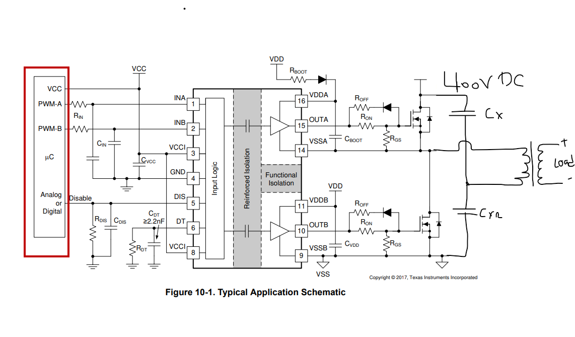
I want to design an isolated half bridge converter 400VDC to 500V AC. The IC of interest is the UCC21520 - isolated dual-channel gate driver evaluation.

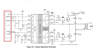
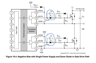
I want to use a single power supply configuration and generates negative bias through a Zener diode in the gate drive loop as shown in page 32 figure 10-4.  However, this IC have two inputs INA and INB, but I want to use a single PWM to drive the input. I see that page 23 Figure 10-1 provides a configuration to drive the two inputs with a PWM controller. (Figure 1 attached)

  • Will PWM controller such as LM5039 - Half-bridge PWM controller with advanced current limit (voltage control) be suitable for such application. The Frequencies can be adjusted from the RT pin while maintain 50% duty, which is suitable for the single power supply configuration of the UCC21520 IC as mentioned in page 32, Figure 10-4.
  • I need options on how to digitally control the RT pin of the LM5039. I am considering using a I2C device pot such as a Digital Potentiometer ICs 50K I2C single 7-bit volatile memory, SOT-363 Microchip Technology Part number MCP4017T-503E/LT. Will it be suitable to control the Frequency of the PWM controller – LM5039? If not, what other options are available?
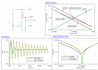
  • Regarding the single power supply – example 3 in the datasheet, what are the important of the components circled in blue-colour? I see that the schematic application in page 23 Figure 10-1 does not have it. (Figure 2 attached). Is it needed?
  • Finally, will the Figure 1 (attached) work with the abovementioned descriptions?

Your comments, recommendations and evaluation boards are welcomed.

Kind regards,

  • Also, do you have evaluation board for Half bridge converter with double ended transformer coupled gate drive?

  • Correction: Instead of a PWM controller such as LM5039, I would prefer something simple such as UCC28083, which offers what is needed. Thank you

  • To be precise - A PWM controller UCC28086D.

  • I forgot to mention that the operating frequency is 25kHz - 40kHZ

  • Hi Bright Robert,

    Please use the UCC21550 instead. It contains many important bug fixes vs. the UCC21520.

    1. You can use the LM5039 or UCC28086D to generate the input to the UCC21550, but make sure you attenuate the HO and LO voltages down to the 5V input level of UCC21550's INA and INB. You can keep the LM5039 completely on the low voltage side. You will need external isolated bias supplies for the output channels of the UCC21550 to support a 500V output.

    2.  That sounds possible. Just verify it will have correct resistance control with a 2Vdc applied.

    3. You should not use Figure 10-4; it has dicey start-up overvoltage. Just short those components out and use the rest of the circuit with a single supply. A tight turn-off Vgs loop is more important than a negative turn-off voltage.

    4. I don't see your figure 1 attachment.

    Maybe you should try and order a UCC28086D EVM and get familiar with that device at a lower voltage level before you try and build this compound system. I am not very clear on what can go wrong with that device, and you might want to reach out to their product line with an E2E post.

    Best regards,

    Sean

  • Hi Sean,

    Thank you for your reply.

    1) I will use the UCC21550 and UCC28086D. Please below the attached figure

    The attached figure is the intended application. I will use the UCC28086D as the PWM controller, it has an output voltage of 4.3V, which is suitable for the UCC21550. 

    1b. The UCC21550 IC has given three different examples of external isolated bias supplies for the output channels of the UCC21550 to support a 500V output. I am considering using the third example as shown in page 33- Figure 8-4 of the datasheet, since the UCC28086D will be operating at 50% duty cycle. Is this the best option?

    1a.  Given my application of the UCC28086D, is it suitable to i) Pull up the CRTL to the VDD with 5k -10k resistor? ii) Pull down the CS pin with 1k resistor?

    2) Are you referring to the VDD (supply voltage) of the digital potentiometer? (Part number MCP4017T-503E/LT, Microchip Technology) It has an operating supply voltage of 1.8V - 5.5V. The voltage on the A and W pin of the pot are VDD +0.3V. 

    3) Just to confirm not to include those components in blue-coloured below. 

    4) Figure 1 is the first figure above. 

    Thank you for your recommendation. 

    Kind regards,

    Bright

  • 5) Regarding isolated power supply for UCC21550, is it suitable to use auxiliary winding of a flyback transformer to bias the external isolated power supply? Instead of having a new isolated power supply. 

  • Hi Bright Robert,

    1b. bootstrap_circuit_negative_turnoff.TSC

    The problem is that the Cz has to charge. If it is too large, you will apply too high +V for a few cycles. If it's too small, then it forms a divider with the FET Cgs, and your output range goes down. Instead I recommend a small transformer and a push pull driver with the SN6501. That will give you the right supply voltage.

    1c. No, you will still need to use this pin for feedback. You will need to "trick" the device into thinking it is regulating a lower voltage.

    2. Great! 2V is the voltage that the IC will apply to the resistor, when it senses the DC current.

    3. Confirmed, refer to my 1b image for my reasoning. This circuit either gives too much positive voltage (transient) or too little negative voltage, for high and low Cz respectively.

  • Hi Sean,

    Thank you for your reply, it is very insightful.

    I am not sure that I understood the point made about the small transformer and a push pull driver with the SN6501. Point 3 is understood, no need for those components circled in blue colour as mentioned about. 

    I need  clarification  regarding the recommendation that you made on a push pull driver with the SN6501.

    1) Are you referring to power supply to the isolated side of the gate driver (UCC21550)? 

    2)  If the answer to 1) is no, Will 16V auxiliary winding of a flyback transformer  suitable for power the isolated side of the IC? 

    3) Do I need to  use a pull driver with the SN6501 to supply those voltage rails to the Isolated side?

    Kind regards,

    Bright

  • Also, regarding Point 2) Great! 2V is the voltage that the IC will apply to the resistor, when it senses the DC current.

    The digital potentiometer voltage at the pin will be VDD (2V) =0.3V. Will that be okay? On the datasheet, it says that RT voltage is 2V absolute. 

    Kind regards,

    Bright

  • Also, if the 2.1 -2.3V is not possible due to the absolute rating on that pin, can I use a zener diode between the RT pin and the digital potentiometer pin W to clamp the voltage across those pins to 1.8V - 2V? 

  • Hi Bright,

    1. Yes. 

    2. Even so, you can use a flyback, but it will take up more room.

    3. you need to use the SN6501 to drive the primary of a small transformer, and you rectify the secondary to get your 16V gate driver supply rail.

    4. RT pin voltage looks like 1.5V typ from last line on page 3. Looks okay to me.

    You should probably order and EVM for the UCC28086 and see what you need to do with the RT pin in a lower voltage test. You can probably ask another E2E question with that device highlighted to get to the experts for that device. I don't think you want to put in a series zener, you should just use that digital potentiometer.

    Best regards,

    Sean

  • Hi Sean, 

    Thank you for the reply.

    2) I am already using a flyback transformer to supply 12V and 5V to  other devices. Hence , I thought about using its auxillary winding to provide isolated power to the gate driver instead of using the SN6501, just to reduce component count. . 

    3) I guess The aux winding seems suitable. 

    4. Okay. I will supply the digital pot with 2V VDD and hopefully it will work. 

    6) Meanwhile, do you have any info on how to calculable the values of a snubber circuit (RC) for a MOSFET in half bridge configuration?

    Kind regards,

    Bright

  • Hi Sean, 

    Question: 1a.  Given my application of the UCC28086D, is it suitable to i) Pull up the CRTL to the VDD with 5k -10k resistor? ii) Pull down the CS pin with 1k resistor? 

    1c. No, you will still need to use this pin for feedback. You will need to "trick" the device into thinking it is regulating a lower voltage.

    -I take that you are referring to the CS pin of the UCC28086D IC? 

    See the Figure below. The PWM controller is the UCC28086D IC in Red coloured rect-box. 

    1) Where can I connect the CS in this configuration? 

    Hence, considering connecting 1k r between the CS pin and GND. 


    Kind regards

  • Hi Bright Robert,

    I can help you with the snubber! The most important thing to remember is that the switch node is always connected to one suppply. High amplitude ringing often appears on the supply too. You can snub this ringing with a snubber across the high voltage bus, without having to cycle the snubber capacitor every cycle. This saves a lot of power vs. a snubber on Vsw itself. An electrolytic capacitor can give you a high ESR and also a high power rating and the right selection can be a very good snubber. Since they have a shorter lifetime than most electronic components, they are often replaced with Tantalum capacitors with many power resistors in parallel.

    You have to measure the switch node ringing frequency, and than estimate the parasitic Csw and Ld values. The FET datasheet can give you a good estimate of the Cds of the FET, and you can add some extra capacitance for the estimated board parasitics. You can then solve for Ld with the equation (2*pi*f)^2=1/LC.

    You can then plot both these L and C impedances on a Bode plot. The intersection will tell you how much resistance is needed to dampen the resonance.

    Once you add this on the HV Bus, you might need to adjust it and monitor the effect on overshoot to account for imprecise estimation of Csw and Ld.

    You might still have some high frequency, low power resonance on the switch node.  For this you can use a much smaller 0603 resistor snubber. You can use the same process as above, but now you have to limit your capacitor size, since it will cycle with the switch node. The CV^2 * fsw must stay below the power rating of the resistor. Then, you can use the bode plot process below to pick a resistor that makes your snubber and Csw parallel look as resistive as possible at the resonant frequency.

    Best regards,

    Sean

    GateRing3 - autosave 23-11-29 11_36.TSC

    Can you please start a seperate E2E question thread for this question pertaining to the UCC28086D?

  • Hi Sean,

    Thank you for the reply.

    Kind regards,

    Bright