This thread has been locked.

If you have a related question, please click the "Ask a related question" button in the top right corner. The newly created question will be automatically linked to this question.

LM66200: Reverse current protection question

Part Number: LM66200
Other Parts Discussed in Thread: TPS2117

We are designing a system using the LM66200 where a DC power supply is connected to VIN1 and a primary Lithium battery is connected to VIN2. When the DC supply is higher than the battery voltage it powers the system on VOUT otherwise the system is powered by the battery. The safety requirement is that any battery charge current (reverse current out of VIN2) must never exceed 25 mA.

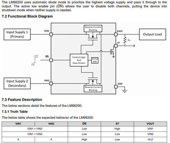
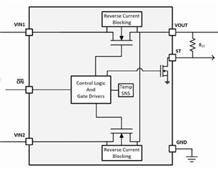
 Referring to the block diagram:


My question regards how the LM66200 functions.

 Is it, as the datasheet suggests, based on ideal diode Or-ing whereby there may be reverse current up to IRCB, Reverse current blocking activation current = 1.4 A typ before VIN2 is deselected and VIN1 is selected (and which could theoretically continue above 25 mA for an extended time before the selection change)?

 Or is the input selection based on voltage comparison between VIN1 and VIN2 and once one input is selected, the other input is blocked in both forward and reverse directions such as with controlled back-to-back FETs. (which is not reflected in the block diagram, and in which case what is the need for the reverse current blocking function).

  • Hi Shawn,

    The second understanding you presented is correct - when one channel is active, the other one automatically blocks forward and reverse current. The input selection is based on VIN1 and VIN2 comparison, and during switchover the active source is disconnected before the other source is connected so no cross-conduction happens.

    The IRCB specification only applies to if there is a voltage source on VOUT that is higher than VIN1 and VIN2, and causes current to flow from VOUT to the active VIN. In that case, if 1.4A typ flows from VOUT to VIN, the device will turn both channels off (Hi-Z).

    Thanks,

    Patrick

  • Hi Patrick, I'm sorry but I'm not convinced on that, the block diagram shows no VINx voltage sensing to the control block. And this FAQ seems to apply to this part. e2e.ti.com/.../faq-tps2117-why-isn-t-my-power-mux-blocking-reverse-current-voltage

  • Hi Shawn,

    Please see the paragraph above the block diagram and the table below it, the two channels' voltages are compared against each other which determines which input is connected to the output. Understood that the block diagram doesn't show voltage sensing, but the descriptions detail this behavior succinctly.

    The FAQ applies to this device (or any of the power mux devices) only if there is a voltage source on VOUT which causes reverse current to the active input, as it details. With these devices, there is no absolutely no cross-conduction between channels - so, as long as you don't have a third voltage source on VOUT that could be higher than the battery voltage, you won't have issues with current flowing out of IN2.

    Thanks,

    Patrick

  • Hi Patrick,

    As I read the paragraph above the block diagram it describes using automatic diode mode, no mention of channel voltage comparison. The truth table can be upheld in either case. We will need to do some testing to confirm. Thank you for your time.

  • Hi Shawn,

    For your extra consideration, please see TPS2117 (data sheet), which is a very similar device with expanded control features. LM66200 is functionally very similar to this device in the "automatic" mode of Table 7-1. This device details the voltage comparison presence in the device, and LM66200 likewise includes the same voltage comparison presence on the inputs.

    Thanks,

    Patrick