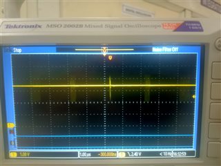
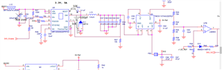
This thread has been locked.

If you have a related question, please click the "Ask a related question" button in the top right corner. The newly created question will be automatically linked to this question.

LMR14050-Q1: LMR14050SQDPRTQ1

Part Number: LMR14050-Q1

Hello 

I am using LMR14050SQDPRTQ1 buck converter in my project in below specification.

Input-28VDC

Output-3.3V/5A

Issue- When I am increasing load 0.1A to upto1A then LMR14050SQDPRTQ1 has gone.
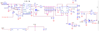
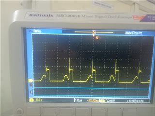
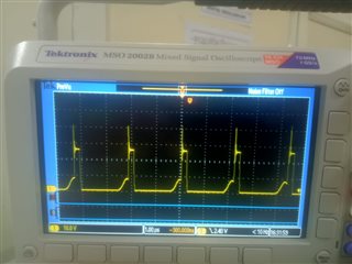
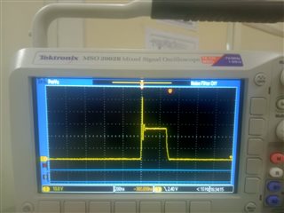
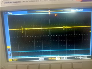
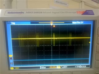
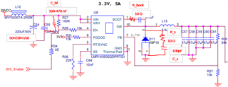
  • Hi Singh,

    Can you please describe the behavior of the part when increasing load from .1A to 1A? Please also send me:

    1. oscilloscope traces of the affected signals as well. SW node voltage, output voltage, and inductor current may be helpful depending on the problem you're seeing

    2. schematic diagram and pcb layout

    Regards,

    Ryan

  • Hello

    Please Find picture circuit and layout.

    When Power on No load condition output voltage coming 3.305VDC and increase load 0.4A Output Voltage is constant.

    When increase more load then LMR14050SQDPRTQ1 has gone bad condition.

    I have seen IC input terminal is short and some time burn IC input pin

    That time I have no seen oscilloscope graph

  • Please see circuit any issue in circuit.

    Suggest me.

  • Hi Vishwanath,

    I will review your circuit and return with suggestions as soon as possible

    Best,

    Ryan

  • Okay

    Please as soon as possible

  • Hi Vishwanath,

    I don't see anything immediately problematic with your schematic. However, can you please clarify how 3V3_enable operates? What is the input source and is it open drain? Additionally, is the 3V3 rail with R31 used to pull up PGOOD? Are you using the signal PGOOD in your system?

    Can you please isolate the LMR14050SQDPRTQ1 from the other IC's and run the test conditions that cause the circuit to fail? What do you mean when the circuit is in bad condition? Does the output voltage stop regulating at 3.3V? Which IC input do you observe burning sometimes?

    Best,

    Ryan

  • Hello

    1. However, can you please clarify how 3V3_enable operates -  I am useing 2 seperatue PCB in my Project. This singal is open in This Board.This Signal 3V3_enable is connect only berg Strip connector

    2. What is the input source - Input Source 3 Phase 115VAC

    Input Source 3 Phase 115VAC------ Rectifier Circuit-------Holdup capacitor--------DCM4623TD2H31E0T70(28VDC)------ LMR14050SQDPRTQ1

    3.Are you using the signal PGOOD in your system?- No

    As per datasheet I am connection output voltage through resistance PGOOD Pin

    4.Can you please isolate the LMR14050SQDPRTQ1 from the other IC's and run the test conditions-  Which  IC

    I am on this IC only LMR14050SQDPRTQ1 other IC connection removed

    when I am increase load(atleast 0.6A) IC start heated.

    5. What do you mean when the circuit is in bad condition- IC is going damage condition.Input Pin is shorting

    6.Which IC input do you observe burning sometimes-Yes

  • Please find wavefrom SW Pin and Output voltage graph with Noload,100mA and 300mA Load.

    Increase Load IC temperature increase.

  • Hi Vishwanath,

    Please ensure your inductors are not saturating.

    Also, in order to isolate the EN signal, please switch R28 and R34 in your schematic. Tie 3V3_Enable to ground so R27 and R34 form a resistor divider from Vin to EN. This will ensure the problem is not coming from the EN input source.

    Best,

    Ryan

  • inductors are not saturating.- No Inductor is not saturating

    Other Point I will work and update on Monday

  • Tie 3V3_Enable to ground so R27(100K),R28(0E) and R34(10K) form a resistor divider from Vin to EN.LMR14050SQDPRTQ1 is starting heat after approx 2Min

  • The overshoot on switch node exceeds the device tolerance for maximum voltage stress. You need to dampen the output using a couple of additional components. In this case, a small resistor (try 5 ohms first, then maximum 10 ohms) in series with C53 from BOOT to SW. Next, add an RC branch from SW to GND close to D11, recommended 100pF in series with 1k ohm each 1206 package. Lastly, please ensure C54 has moderate ESR. Another pair of high frequency input capacitors (100nF) is recommended as close to each Vin pin as possible.

    I hope this helps,

    Ryan

  • Apologies, Vishwanath. Please use a 10 ohm resistor instead of 1k ohm. in the snubber across D11

  • Can you explain to me by drawing a schematic or graph?

  • moderate ESR on C54: >50mOhms.

    C_hf should be small package smaller than 0603 and close to Vin input pin.

    Use a larger package 0603 or larger for R_s and C_s. 

    R_boot looks good in your depiction