This thread has been locked.

If you have a related question, please click the "Ask a related question" button in the top right corner. The newly created question will be automatically linked to this question.

UCC14140-Q1: Paralleling Gate Drive PSU Inputs for a Three Phase Two-Level Inverter and Common-Mode Current Mitigation

Part Number: UCC14140-Q1

Hello,

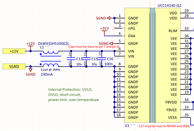
We're working on updating our gate driver design for our three-phase two-level SiC inverter to utilize the UCC14140-Q1 and I had a question about paralleling the inputs and common-mode provisions. We previously used a common-mode choke on the 12V input to damp any common-mode currents that traveled across the isolation capacitance in the high-side PSU due to high dv/dt (10-20V/ns) on the switch node. See image below. 

However, when using the UCC14140-Q1, this creates a problem. This means we cannot connected the GNDP pins to the SGND plane for heatsinking. 

What is the recommended solution here? Is the common-mode choke unnecessary? I don't see any recommendations in the datasheet for it.

One thought we had was to have LC filters on the GD PSU inputs to to avoid diff noise coupling between the PSUs and then have a single common-mode choke on the 12V input to prevent CM current from getting into switching converter that is producing the 12V role. This would allow us to tie the GNDP pins to the SGND planes for heatsinking, but CM current could still aggress from one PSU to another. Is this an issue?

Thanks,

Jason

  • Jason,

    Great questions - you are hitting on two of the most important concerns for IIB (Integrated Isolated Bias) modules: thermal performance and EMI mitigation. For thermal, you are correct, the most important thing to know is what is detailed in section 9.5 of the UCC14141-Q1 data sheet, specifically what is highlighted below:

    The above example and the EVM do not take into account EMI filter components and as you pointed out, the challenge to make a suitable heatsink can be difficult when SGND and GNDP are separated by EMI components. You need to provide copper around GNDP and VEE pins to act as a heatsink. This means you may need to extend copper, as much as possible around GNDP and add thermal vias connecting into internal parallel GNDP plans and/or bottom side external GNDP plane. Thermal relief (vias and/or plated though-hole spokes) may be good for manufacturing purposes but is counter productive for heat extraction. Attached is also some proven effective EMI filter design guidance.

    EMI MagnetoMV_CE Filter_Customer Share.pdf

    Regards,

    Steve

  • Thanks Steve. If you were to have 6 of the optimized circuits shown on page 4 of the PDF you sent, would you have the GNDPs connected of all 6 PSUs connected together or isolated from each other?

  • Hi Steve, Does the TINA simulation for this component accurately reflect differential and common mode current on the input?

  • Inputs are all common. Also, the EMI approach I shared is for a single UCC14xxx. For 6x UCC14xxx, you may be able to use a single CM choke that is rated for the current required from 6x UCC14xxx. I have not tried this approach yet but I believe it's feasible and if you use a single CM choke, maybe then you add the DM filter and X2Y caps at the input of each UCC14xxx. 

    Steve

  • We do not have a TINA sim for UCC14140-Q1. We are offering a sim model for SIMerix/SIMPLIS and this requires the full licensed version to run but even this is only behavioral. With the behavioral model you may be able to run a time domain transient analysis and then use FFT but I would say this will likely not be an accurate representation of the actual converter module.

    Regards,

    Steve