This thread has been locked.
If you have a related question, please click the "Ask a related question" button in the top right corner. The newly created question will be automatically linked to this question.
Hello,
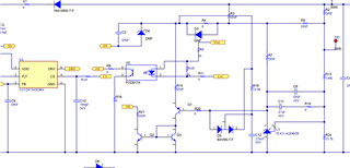
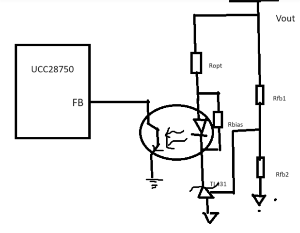
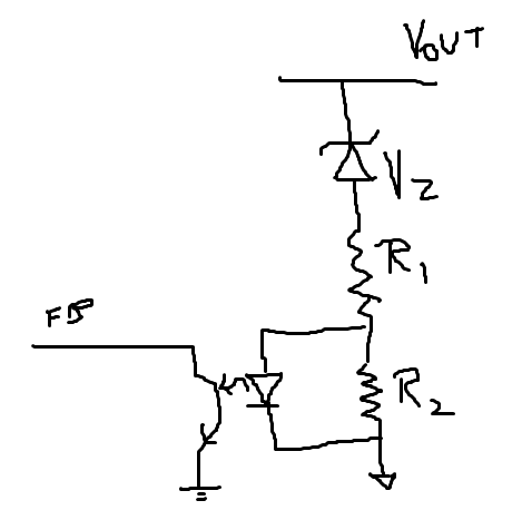
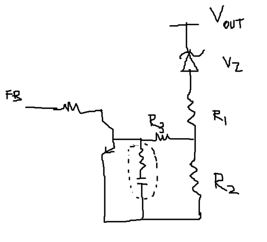
We're working on a UCC287505 flyback design.
One version of the solution is AC input and we need to isolate the secondary.
however a different version is using low voltage DC input and it would be nice to be able to remove the opto coupler need and several passive components. (can ATL431 be removed as well?)
Is there a way to hook up this IC so that we can directly control the FB?
Thank you, Keith
Hi Keith,
This circuit was developed by PDS team and can be used for non isolated design.
If I remember correct there is a reference design PMP31288 developed by PDS team, not sure if it is released, but definitely it can be used.
Also shown below is another knaive version with a zener and npn
Q1 goes to the FB pin which can be used to control.
Thank you
Regards,
Harish
Hello,
Could you please provide more details on the circuit:
Thank you, Keith
Hi Keith,
I do not have very fine details. I had tried this on a high Voltage buck circuit based on UCC28750.
Thank you
Regards,
Harish
Hello Harish,
Would it be possible to simulate the difference in Vout load regulation based on using your circuit versus an opto coupler?
Thank you, Keith
Hi Keith,
It will be difficult to simulate the cases to check voltage regulation difference as a lot of these depend on the choice of feedback components (their modelling). So it is better to implement this on the board but let me try to explain how this is implemented so customer can try to verify at their end.
Shown below is the implementation for UCC28750 using TL431. In all cases GNDs can be changed for non isolated configuration.
Now in the above we can replace TL431 with zener diode as shown below:
The series drops across Vz, R1 and the forward drop of the LED of opto determine the output voltage. A diode is optional depending on the availability of a suitable Zener voltage. Resistor R2 provides a 0.5 mA bias current so that Vz is operated close to its knee voltage. Resistor R1 adjust the output voltage and limits the feedback current during output load transient.
Vout = Vz+Vopto(forward drop)+VR1
Output regulation is fully dependent upon the choice of these components but I thinkTL431 based scheme offers better regulation.
Lastly,
R2 basically is selected to set the bias current in Vz. R3 limits the base current to the transistor, the dotted components are optional which decide the roll off of high frequency gain.
Thank you
Regards,
Harish