TPS552892: Efficiency does not meet specifications(5Vin/ 5vout)

Part Number: TPS552892

When I tesing my design board for TPS552892.

The efficiency does not meet specifications definition.

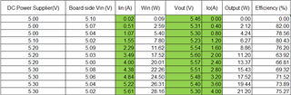
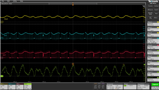
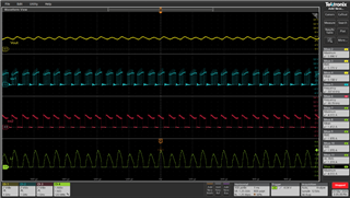
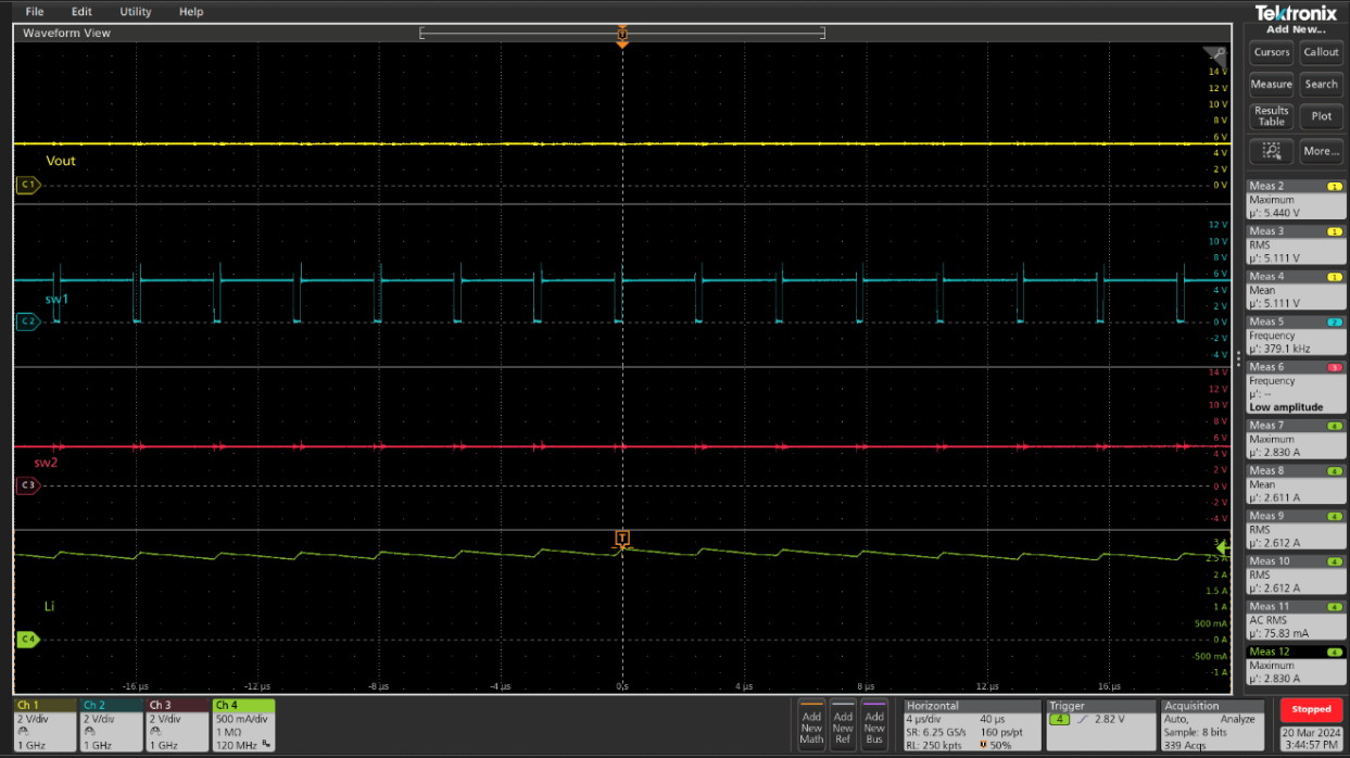
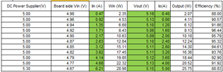
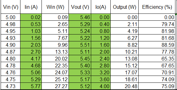
Test data1 _(PFM_5Vin/ 5vout):


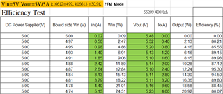
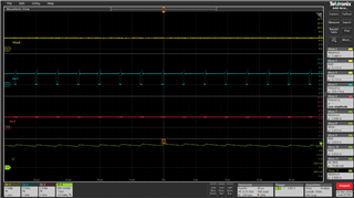
Test data2 -(FPWM_(5Vin/ 5vout)):


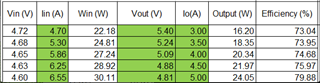
But, When I change the VIn to 20V(Keep Vout : 5V)

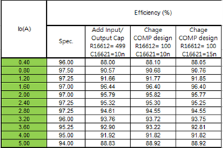
The measurement data is close to the specification information.

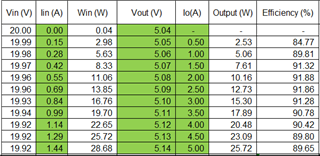
Test data2 -(FPWM_(20Vin/ 5vout)):


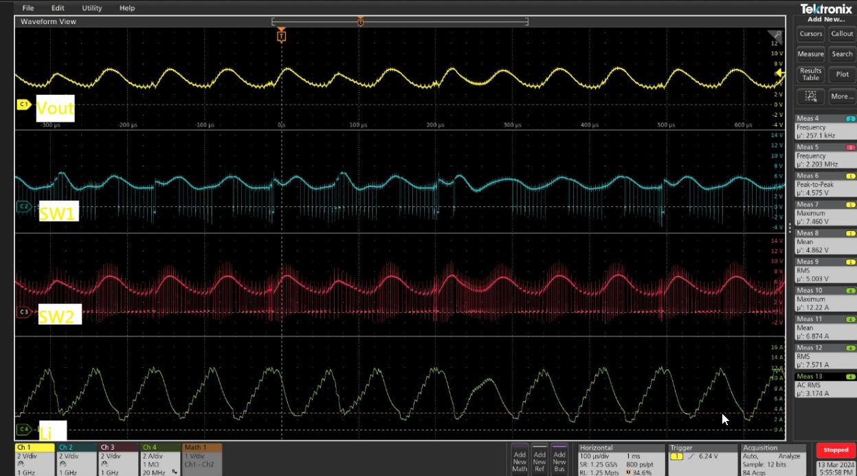
As far as I know, 558892 d uty cycle can be 100%,

Why is it so bad of Efficiency for 5vin/5vout?

  • Hi Eugene,

    Thank you for reaching out. May I know how did you test the efficiency? Did you test the input voltage and output voltage as close as to the chip? As to your test result, I think it may be caused by wrong measure method. When Vin=5V, input current is large and there will be voltage drop between power supply and the chip because the wire has resistor. As you can see, the larger the input current, the larger the voltage drop,  the smaller Vin test result.

    You can try to test the voltage across the input/output ceramic capacitors. Make sure the input voltage close to chip is 5V, which means when load increases, you should slightly increase the power supply voltage to compensate the voltage drop cause by the  wire resistor.

    Let's see the efficiency result under this test method.

    Regards,

    Mulin

  • HI Mulin

    Thank you for your answer.

    Regarding the voltage, I directly confirmed the value with the VOM meter, measuring it at the end of the board close to the IC.

    And tested through the power supply and load (separate TPS5528922 power module circuit)

    After your reminder, I re-verified to ensure that the voltage on the board meets 5V.

    But, the result still fails to meet the specifications.

    In addition, I perform waveform measurements (Vout/ SW1 / SW2 / Li )
    When the load exceeds 2A, the waveform will appear abnormal, but I don’t know why.

  • Hi Eugene,

    It seems that system is not stable. Can you help check Vin waveform? Does power supply reach current limit?

    Also please provide schematic and layout file so that I can check if the design is reasonable. Please provide part number or datasheet of the output capacitors(ceramic and electrolytic) and inductor. What is the input voltage, output voltage, output current range?

    Regards,

    Mulin

  • Hi Mulin

    Could you help to provide the mail address?

    I will send the data  to you.

  • Hi Eugene,

    My mail address is: mulin-yuan@ti.com

    Regards,

    Mulin

  • Hi Eugene,

    The waveforms shows the system is not stable when Vin=Vout=5V. According to my calculation, current compensation parameters leads to phase margin<0. Please change R16612 to 500ohm to see if the system can be stable.

    Currently, there is only ceramic capacitors in output side. May I know why don't you add an electrolytic capacitor? This will cause: 1. Relatively large undershoot and overshoot in transient conditions. Do you have any requirement in undershoot and overshoot voltage. 2. Difficult for compensation calculation. Please kindly let me know your opinion.

    Also, just check that in schematic, R16613 is 30.1ohm, which should be 31.5k. 

    I will wait for your update.

    Regards,

    Mulin

  • Hi Mulin,

    We had 100uF aluminum capacitors placed close to the device end, although they are not shown in the schematic. We suspect that the short pulse loading generated from devices could be mitigated if we place the capacitors close to the device side. However, during the power efficiency test, we removed the short lands. Therefore, in the power efficiency test, there are no electrolytic capacitors present.

    We will check the results after replacing R16612 and R16613 and report back to you later.

    Thank you.

  • Hi Eugene,

    Thank you for your feedback. I recommend R16612 = 500ohm based on that there is no aluminum capacitor. After doing the efficiency test please modify the compensation parameters again. 

    Regards,

    Mulin

  • Hi Mulin,

    Thank you for your feedback.

    After testing, the efficiency has been significantly improved, when i change the R16612 and R16613.

    Since I don’t have a completely matching resistor value at hand, my modified parameters are as follows,

    R16612= 499ohm / R16613= 30.9K

    However, there are still some values ​​that deviate from the specifications.( 0.8A & 2A & 4A)

    I focus special attention to the situation of the waveform outputting as below,

    Load = 0.8A

    Load= 2A

    Load= 4A

    For these deviation states, are there any steps we can take to improve?

    Also, have you seen any problems with the layout?

  • Hi Eugene,

    Can you provide waveforms of  specifications :1.2A & 2.4A & 3.6A? I want to check the comparison of the normal and abnormal situation.

    Can you provide the part number or datasheet of the 100uF aluminum capacitor? If the system stills shows instability, maybe we can try to add the 100uF aluminum capacitor and modify the compensation parameter in the next step. Show me the above waveforms first.

    I will give you layout feedback later today.

    Regards,

    Mulin

  • Hi Eugene,

    Please see my feedback about layout.

    1. It seems that GND pin of the device is not connected to the GND panel. Please check the original file.
    2. Add a GND panel as blue line mark. Do not add vias in the pad. Put the vias in the panel.
    3. Put Vin and Vout 0.1uF capacitor as close as to the device as the green rectangle shows. Also put vias in the panel, not the pad.


    4. SW2 RC snubber is not connected. Please check if it is just deleted in this file.


    5. Do not put vias in the signal component pads. This will cause parasitism problem and soldering reliability problem.


    6. About PGND and AGND connection:


    7. About thermal performance:


    8.What is the part number of R16606? I am curious about the package.

    Regards,

    Mulin

  • Hi Mulin,

    Update the test waveform as below.

    and, I will give you the data for capacitor by mail.

    1.2A

    2.4A

    3.6A

  • Hi Eugene,

    From my opinion, the system is not stable now, so the efficiency can not meet specifications definition. About the above waveform, only the 2.4A test condition is stable. We can optimize compensation parameters or change output capacitors to improve.

    1. Just double check that GND pin of the device is well connected as the layout review says.

    2. With only C16611-C16616 populated(no electrolytic capacitors), reduce R16612 value (from 500 to100) and check if system is stable as below. Also you can slightly increase C16621 value(from 10nF to 15nF). Calculation result is just for reference. We need to adjust compensation parameters by experiment.

    3.If adjust the compensation parameters can not help, then add the two 100uF capacitor(try 500ohm + 10nF compensation parameters first). ESR of the capacitor is large(1.7ohm) and this will reduce efficiency and make it difficult for compensation. Can you consider to change to electrolytic capacitors with ESR<60mohm?

    Look forward to your feedback.

    Regards,

    Mulin

  • Hi Mulin,

    After testing, the measured waveform became stable, When I rework to adding the electrolytic capacitance of Input/Output!

    The status of the test is as follows.

    R16612= 499, R16613 = 30.9K , Input add Cap for 100uf , Output add Cap for 100uf*2

    We get better efficiency, and close to the specification definition.


    Additionally, I tried replacing the resistors and capacitors(R16612 & C16621) and keep Input/output Cap as above.

    But , efficiency not much change.

    Update information for you,
    Best wishes,

  • Hi Eugene,

    Glad to hear that the efficiency is stable now. So we have find the cause of low efficiency:

    1. The loop is not stable. Only with electrolytic capacitance  can solve this problem。

    2. Even though the efficiency is stable, it is still lower than spec. I am afraid that using capacitor with so large ESR, it is obvious that the efficiency is lower than our EVM. Also you can compare DCR of the inductor. 

    So please make sure loop is stable and use smaller ESR capacitor and low DCR inductor. 

    Regards,

    Mulin

  • Hi Mulin,

    For #2, we will confirm the ESR and DCR differences between EVB and ours.

    Thanks.