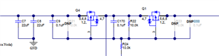
When VBUS is 5V, the gate voltage on the back-to-back P-channel enhancement MOSFETs is only 2.5V. This results in the two transistors having a net resistance of 0.21 Ohms. This results in 2W of power dissipation in the transistors at 3A current draw. Changing R22 and R34 to 100k results in an acceptable Rds on of 0.05 Ohms for the two transistors combined. This however creates a new problem in that the RC constant is changed. In our system power can come in on port 1 from a PC, then if a higher power source is offered on Port 2 it will switch to that port. When switching to a higher voltage port 2, C10 would keep the gate voltage from rising with the system voltage and Q1 would be partially on, connecting the higher voltage back to VBUS on port 1. This situation unfortunately damaged a PC and a USB hub during development in our office. The solution is to remove C10. What is the reason for C9 and C10? I seems as though the design has less risks of problems without them.

-
Ask a related question
What is a related question?A related question is a question created from another question. When the related question is created, it will be automatically linked to the original question.