Hi team,
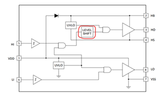
Can you provide the data for UCC27211A-Q1 related to total gate charge needed by internal level shifter to operate?
Best regards,
Foong Wei Seng
This thread has been locked.
If you have a related question, please click the "Ask a related question" button in the top right corner. The newly created question will be automatically linked to this question.
Hi team,
Can you provide the data for UCC27211A-Q1 related to total gate charge needed by internal level shifter to operate?
Best regards,
Foong Wei Seng
Hey Foong Wei Seng,
Thank you for your question regarding the UCC27211A-Q1.
Are you asking about a minimum gate charge for the power FETs? Or are you asking about internal specifications of the level shifter?
Thank you,
William Moore

Customer want to know the total gate charge for the level shift in the UCC27211A-Q1 to calculate the power dissipation in the gate driver theoretically.
Hey,
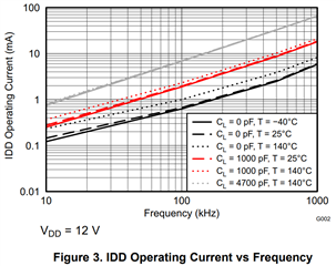
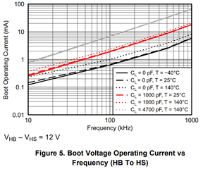
We do not have a spec for this but the power dissipation for the gate driver can be calculated and determined using the quiescent current and the no load operating current at the desired frequency to determine the power dissipation of the gate driver itself.
The power dissipation calculations are seen in Section 9.2.2.5 Power Dissipation in the datasheet.
Let me know if there are any further questions.
Thank you,
William Moore
Hello,
You said the power dissipation for the gate driver can be calculated and determined using the quiescent current and the no load operating current at the desired frequency, but there is no explanation for the loss of no load operating current at the desired frequency in Section 9.2.2.5.
I can only see the loss from the quiescent current and gate charge as shown below.


Then, could you answer the following questions?

3. I wrote down a equation for the loss of the gate driver below. Is it correct?
When a gate driver is not switching: P = (IDD+IHB+IHBS)*VDD
When a gate driver is switching: P=(IDDO+IHBO+IHBSO)*VDD + Qg*VDD*Fsw (gate charge loss)
Best regards,
Foong Wei Seng
Hey,
1. For the operating current, please refer to Figure 3 and Figure 5 in datasheet Section 7.7 Typical Characteristics.


2. For the quiescent current and operating currents, you need to factor in all 3 currents for each condition.
3. For these loss equations, these equations are correct.
Thank you,
William Moore