This thread has been locked.

If you have a related question, please click the "Ask a related question" button in the top right corner. The newly created question will be automatically linked to this question.

BQ76952: When the OCD1 threshold is reached, both the OTPB will reset and partial analog data will reset to default value.

Part Number: BQ76952

Hello team,

We are currently utilizing the bq76952 in our product, and we've encountered an unexpected issue during our testing phase.

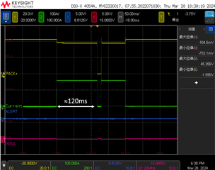
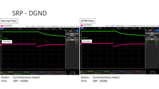
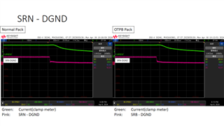
While testing the OCD1 protection feature, we observed some unexpected behavior. Specifically, when the current reached approximately 263A, the value of the [0x12] Battery Status Register transitioned from 0x0180 to 0x0100. This indicates that the OTPB bit was reset. Concurrently, the cell voltage reading became incomplete, with registers 0x1C through 0x26 displaying zero values. Additionally, the temperature reading reset to 273.15.

However, upon turning off the Eload and reducing the current from 263A to 1.2A, the system appeared to function correctly again.

The setting of the OCD1 : { threshold = 152A, delay = 118.8ms }

We have verified the accuracy of our logs using a logic analyzer to parse the I2C signals, confirming that the readings are indeed correct.

Notably, no SET_CFGUPDATE() function was invoked during this sequence.

For clarity, the items referenced in the log file are explained as follows:

  • wSafetyAlertA: [0x02] Safety Alert A Register
  • wSafetyStatusA: [0x03] Safety Status A Register
  • wBQBatteryStatus: [0x12] Battery Status Register
  • OTPW: OTPW bit within the [0x12] Battery Status Register bit-field
  • OTPB: OTPB bit within the [0x12] Battery Status Register bit-field
  • iCell_V1 to iCell_V16: Individual cell voltage readings
  • iSTACK_V: [0x34] Stack Voltage
  • iPACK_V: [0x36] PACK Pin Voltage
  • iLD_V: [0x38] LD Pin Voltage
  • iCC2: [0x3A] CC2 Current
  • iINT_T: [0x68] Internal Temperature
  • iTS1_T: [0x70] TS1 Temperature
  • iTS3_T: [0x74] TS3 Temperature

We appreciate your assistance in resolving this issue promptly.

V0033 OCD-3 UART LOG.xlsx

  • Another hypothesis is that the device triggers a reset when the loading current surpasses the OCD1 threshold. This could potentially explain why the analog data readings reset to their default values, with the voltage dropping to zero and the temperature resetting to -273.15°C.

  • Hello Lin,

    That is indeed very strange. So, the protection triggered in this case? Did you measure with an oscilloscope the board during the OCD event?

    Can you share your schematic?

    Best Regards,

    Luis Hernandez Salomon

  • Hi Luis,

    Please see the attached plot showing when the OCD occurred.

    After the OCD trip, the C/DFET is turned off, and then roughly 10ms later, it is turned on again. We suspect that the bq76952 experiences a 10ms-POR, as evidenced by the log indicating that partial data is unreachable.

    However, we are unsure if our assumption is correct, as the bit POR in the Battery Status register remains unset after the POR event.


    Note: The ALERT pin in the plot can be neglected as we are currently not utilizing the ALERT function.

  • Hello Lin,

    That could be possible. We've seen similar cases when faults trigger. Do you have a schematic you could share? 

    Best Regards,

    Luis Hernandez Salomon

  • Dear Luis,

    Please find attached the circuit diagram related to the bq76952. Do you require any additional circuit diagrams or information?

    You mentioned that you've encountered similar cases before. Could you please provide me with the relevant issue numbers from the forum for reference?

    Additionally, based on your expertise, do you have any insights or thoughts on potential root causes for the issues we are facing?

    Best regards,

    Chia Chun Lin

  • Hello Chia,

    Can you get a waveform capture of SRP pin with respect to IC ground(Vss) and SRN pin with respect to IC ground as well? If these were both to go high with respect to Vss during the turn-off, that may cause problems.

    I cannot recall an E2E off the top of my head.

    Can you share the FET circuitry? If you measure REG18 during this event, how does it look? 

    Best Regards,

    Luis Hernandez Salomon

  • Hi Luis,

    Attached are the FET circuitry and signal plots.

    The timing captured in the plots indicates when the DFET is switched off.

    Here are the key observations:

    1. The behavior of a normal pack triggering OCD1 aligns with our expectations and is consistent with the behavior of the pack that did not trigger OCD1.

    2. REG18: No significant drop or pulse was observed.

    3. SRP - DGND & SRN - DGND: A voltage drop of approximately 200~300mV occurs when the DFET is turned off.

    We obtained an interesting test result during our investigation. When we externally set the RST_SHUT pin to HIGH for less than 1 second, causing a partial reset of the bq76952, and simultaneously polled the bq76952 via I2C for register status and analog data, we observed the same phenomenon (OTPB reset and partial analog data resetting to default values).

    Based on this, we suspect that the bq76952 might be entering a partial reset during the OCD1 test. However, the triggering event remains unknown. We are uncertain why the bq76952 is entering this partial reset state. What do you think?

    Best regards,

    Chia Chun Lin

    ppt_upload_20240408.pptx

  • Hi Luis, 

    I've got an update on our SRP/SRN ground test. Originally, the bq76952 ground was connected to "DGND", which is another ground in our system, instead of "VBAT-". This setup caused a voltage drop of about 200-300mV when the DFET was off.

    We tried shorting "DGND" and "VBAT-" to improve this. The voltage drop reduced to around 50mV, but the overall result remains unchanged from before the modification.

    Best regards,

    Chia Chun Lin

  • Hi Lin,

    Luis is out of office until Wednesday (4/10) and will be able to get back to you then.

    Thank you for your patience.

    Regards,

    Max Verboncoeur

  • Hello Chia,

    What is the voltage division of the waveforms? What are the voltages here? It is a bit hard to see.

    I understand, that is not good, BQ76952's ground should be near BAT-. Usually we connect the high current path of BAT- with a net-tie to the low-current path of the IC ground.

    Something I notice from your images is that SRP seems to be going below ground, how low is this going? Is it also possible to see what is the RST_SHUT voltage throughout this sequence?

    Best Regards,

    Luis Hernandez Salomon

  • Hi Luis,

    Sorry for low-resolution image, I didn't notice that. I re-upload the image that I uploaded two days ago.

    Last plot in the PPT is the RST-SHUT behavior during the test.

    Best regards,

    Chia Chun Lin

    ppt_upload_20240411.pptx

  • Hello Chia,

    No worries! Thank you for the PPT, it is a lot clearer there.

    I am concerned about the negative transient on RST_SHUT, that is going way too negative, going below our absolute mins of the part. Is REG18 also going below ground? If REG18 drops in voltage too much, there could be a POR event, causing a reset of the part. That could explain the turn-off of the FETs as well.

    Best Regards,

    Luis Hernandez Salomon

  • Hi Luis,

    The previous two slides on V.Rsense and RST_SHUT were for clarification; I had uploaded them earlier.

    Regarding the last slide on REG18, the voltage change is minimal and falls within the specified range.

    What concerns me is the observed behavior during our testing of two packs: the normal pack and the OTPB pack (which appears to experience a partial reset and reset the flag- OTPB when the DFET turns off—I'll refer to this as the "OTPB" pack).

    Both packs show similar pin behavior (RST_SHUT/REG18/SRP-GND/SRN-GND/...), but while the normal pack triggers OCD1 as expected with no issues, the OTPB pack undergoes a partial reset. I'm currently unable to pinpoint a clear reason for this discrepancy.

    Best regards,

    Chia Chun Lin

    ppt_upload_20240412.pptx

  • Hello Chia,

    Glad to see REG18 is okay. It worries me that these are going below ground, even -600-mV is already going beyond our abs min specs. 

    Yes, it is hard to know why this may be happening in this pack. What happens if you do this test with an added Schottky to the RST_SHUT pin to clamp the negative voltage?

    Best Regards,

    Luis Hernandez Salomon

  • Hi Luis,


    Regarding RST_SHUT, we attempted to short it to GND during testing, but the results remained unchanged.

    Best regards,

    Chia Chun Lin

  • Hello Chia,

    Apologies that we have not been able to narrow down what may be causing a reset. 

    Could you do a test where SRP is shorted directly to the AFE Vss/Ground and see if there's any difference?

    Also, do you see any other pins that are going to abnormal voltages during the tests?

    Best Regards,

    Luis Hernandez Salomon

  • Hi Luis,

    We conducted a test by shorting the SRP to AFE GND, but the results remained unchanged.

    Regarding the other pin, we found that the cell voltage exceeds the threshold, maybe this is a potential cause? Please refer to the attached document for details.

    We observed that the maximum voltage spike in the cell, occurring when DFET is turned off due to OCD protection, exceeds the 5.5V threshold at certain cell pins. This phenomenon is unique to the OTPB pack.

    In a normal pack, the OCD is induced as expected. However, in the OTPB pack, it results in a partial reset, resetting some analog data to default values (voltage: 0, temperature: -273.15°C).

    Best regards,

    Chia Chun Lin

    ppt_upload_20240416.pptx

  • Hello Chia,

    Does BAT+ do not increase in voltage during this test? It is odd that it seems the VC pins add to a voltage larger than the BAT+ voltage. 

    What is the VC0 voltage on these? Even if the VC pins are going above the recommended, I do not believe it should cause any sort of reset. These pins should be able to handle a VCx to Vss voltage of ~85-V (With the exception of VC0, which is a low-voltage pin).

    It is definitely curious as to why the abnormal unit has a higher voltage on some of these pins.. Have you tried to clamp the voltages with TVS diodes? It could be good to have these before the input filters to attempt to clamp the voltage. and see if there's an improvement

    Best Regards,

    Luis Hernandez Salomon

  • Hi Luis,

    In our previous test, the voltage at the AFE BAT pin remained stable because the capacitors filtered out the voltage spike. Please refer to slide 17 in the attached PPT for details.

    The VCx voltage aligns with the AFE pin definitions. Therefore, the VC0 voltage matches the AFE "VC0" pin voltage, which is connected to AFE VSS.

    Given that the voltage spikes we tested are within the acceptable range, as you mentioned, this may not be the cause of the issue, right?

    We haven't tested the diodes yet but might try this test to see if there's any improvement.

    Best regards,

    Chia Chun Lin

    ppt_upload_20240417.pptx

  • Hello Chia,

    Do let us know how the test goes with the diodes!

    Oh, I just noticed VC0 is connected directly to the AFE Vss.

    This is actually not usually done. We do not connect VC0 directly to Vss typically, it connects through the device's Vss through the filter resistor, in this case being RA14. You can see our EVM schematic for reference. During this test, did you measure the VC0 pin voltage compared to DGND/Vss?

    Best Regards,

    Luis Hernandez Salomon