Other Parts Discussed in Thread: BQ79616-Q1
Hi all,
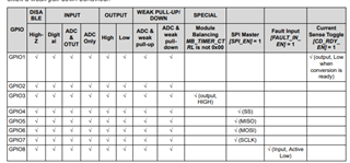
i am working on BQ79656-Q1 and when i use GPIO1-GPIO8 as a only ADC than i get only results on GPIO1-GPIO3 and not getting results on GPIO4-GPIO8
Below is my configuration please help me.
Wake79600(); //send wake ping to bridge device
delayus(3500); //wait tSU(WAKE_SHUT), at least 3.5ms
Wake79600(); //send wake ping to bridge device
delayus(3500); //wait tSU(WAKE_SHUT), at least 3.5ms
//INITIALIZE BQ79616-Q1 STACK
WriteReg(0, CONTROL1, 0x20, 1, FRMWRT_SGL_W); //send wake tone to stack devices
delayms(11.6*TOTALBOARDS); //wake tone duration is ~1.6ms per board + 10ms per board for each device to wake up from shutdown = 11.6ms per 616 board
//AUTO-ADDRESS
AutoAddress(); //auto address sequence
//RESET ANY COMM FAULT CONDITIONS FROM STARTUP
WriteReg(0, FAULT_RST1, 0xFF, 1, FRMWRT_STK_W); //Reset faults on stacked devices
WriteReg(0, FAULT_RST2, 0xFF, 1, FRMWRT_STK_W); //Reset faults on stacked devices
WriteReg(0, Bridge_FAULT_RST, 0x22, 1, FRMWRT_SGL_W); //Reset FAULT_COMM and FAULT_SYS on bridge device
//ENABLE BQ79616-Q1 MAIN ADC
WriteReg(0,CONTROL2,0X01,1, FRMWRT_SGL_W);
delayus(1500);
WriteReg(2, GPIO_CONF1, 0x12, 1, FRMWRT_SGL_W);
delayus(100);
WriteReg(2, GPIO_CONF2, 0x12, 1, FRMWRT_SGL_W);
delayus(100);
WriteReg(2, GPIO_CONF3, 0x12, 1, FRMWRT_SGL_W);
delayus(100);
WriteReg(2, GPIO_CONF4, 0x12, 1, FRMWRT_SGL_W);
delayus(100);
WriteReg(2, ACTIVE_CELL, 0x0A, 1, FRMWRT_STK_W); //set all cells to active
WriteReg(2, ADC_CTRL1, 0x06, 1, FRMWRT_STK_W); //continuous run and MAIN_GO
delayus(200);
do{
ReadReg(2, /*AUX_GPIO_HI*/GPIO1_HI, response_frameA, 2, 0, FRMWRT_SGL_R);
delayus(100);
ReadReg(2, /*AUX_GPIO_HI*/GPIO2_HI, response_frameB, 2, 0,FRMWRT_SGL_R);
delayus(100);
ReadReg(2, /*AUX_GPIO_HI*/GPIO3_HI, response_frameC, 2, 0, FRMWRT_SGL_R);
delayus(100);
ReadReg(2, /*AUX_GPIO_HI*/GPIO4_HI, response_frameD, 2, 0, FRMWRT_STK_R);
delayus(100);
ReadReg(2, /*AUX_GPIO_HI*/GPIO5_HI, response_frameE, 2, 0, FRMWRT_STK_R);
delayus(100);
ReadReg(2, /*AUX_GPIO_HI*/GPIO6_HI, response_frameF, 2, 0, FRMWRT_STK_R);
delayus(100);
ReadReg(2, /*AUX_GPIO_HI*/GPIO7_HI, response_frameG, 2, 0, FRMWRT_STK_R);
delayus(100);
ReadReg(2, /*AUX_GPIO_HI*/GPIO8_HI, response_frameH, 2, 0, FRMWRT_STK_R);
delayus(100);
for(int i=0; i<5; i++)
{
// GPIO 1
uint16 rawDataA = (response_frameA[4] << 8) | response_frameA[5];
float CellvoltageA = rawDataA*0.00015259; //rawData*VLSB_ADC
printConsole("fst gpio---%f\n", CellvoltageA);
// GPIO 2
uint16 rawDataB = (response_frameB[4] << 8) | response_frameB[5];
float CellvoltagB = rawDataB*0.00015259; //rawData*VLSB_ADC
printConsole("2nd gpio---%f\n", CellvoltagB);
// GPIO 3
uint16 rawDataC = (response_frameC[4] << 8) | response_frameC[5];
float CellvoltagC = rawDataC*0.00015259; //rawData*VLSB_ADC
printConsole("3RD gpio---%f\n", CellvoltagC);
// // GPIO 4
uint16 rawDataD = (response_frameD[4] << 8) | response_frameD[5];
float CellvoltagD = rawDataD*0.00015259; //rawData*VLSB_ADC
printConsole("4RD gpio---%f\n", CellvoltagD);
// GPIO 5
uint16 rawDataE = (response_frameE[4] << 8) | response_frameE[5];
float CellvoltagE = rawDataE*0.00015259; //rawData*VLSB_ADC
printConsole("5TH gpio---%f\n", CellvoltagE);
// // GPIO 6
uint16 rawDataF = (response_frameF[4] << 8) | response_frameF[5];
float CellvoltagF = rawDataF*0.00015259; //rawData*VLSB_ADC
printConsole("6TH gpio---%f\n", CellvoltagF);
// // GPIO 7
uint16 rawDataG = (response_frameG[4] << 8) | response_frameG[5];
float CellvoltagG = rawDataG*0.00015259; //rawData*VLSB_ADC
printConsole("7TH gpio---%f\n", CellvoltagG);
// // GPIO 8
uint16 rawDataH = (response_frameH[4] << 8) | response_frameH[5];
float CellvoltagH = rawDataH*0.00015259; //rawData*VLSB_ADC
printConsole("8TH gpio---%f\n", CellvoltagH);
}
}
thanks