This thread has been locked.

If you have a related question, please click the "Ask a related question" button in the top right corner. The newly created question will be automatically linked to this question.

TLC59401: Can't receive MSB of DC data

Part Number: TLC59401
Other Parts Discussed in Thread: TLC5940

When I wrote driver software (python) for TLC59401, I have found that OUT15 LED is less brighter than other.

For all 16 LED, same DC and same GS value send, but only OUT15 LED is about half brightness. If I send DC=32 and any GS value, only OUT15 is not turn on.

I think TLC59401 can't receive MSB=1 of DC data.

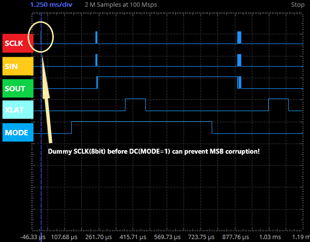
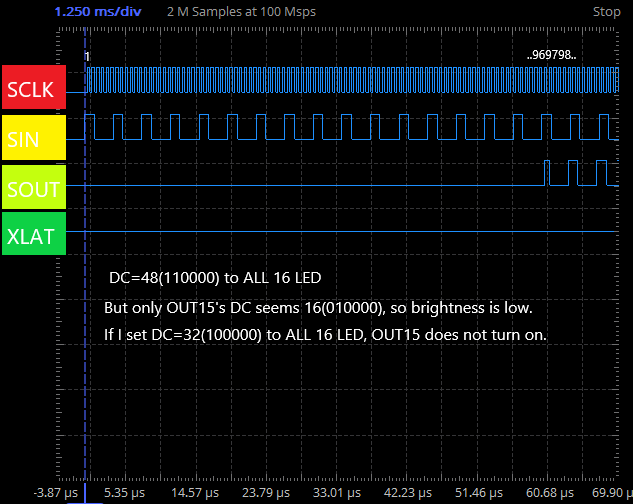
Upper chart is analyzer of SCLK/SIN/SOUT/XLAT. DC=48(110000) to 32 LED(TLC59401 is cascaded) found SIN, but MSB of SOUT seems DC=16(010000), so OUT15 on 2nd TLC59401 is less brighter than other.

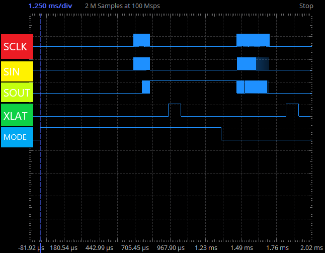
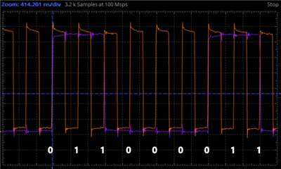
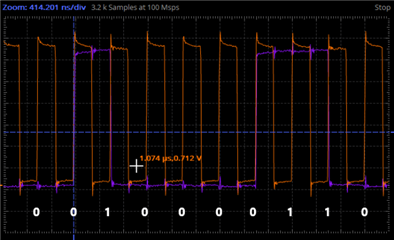
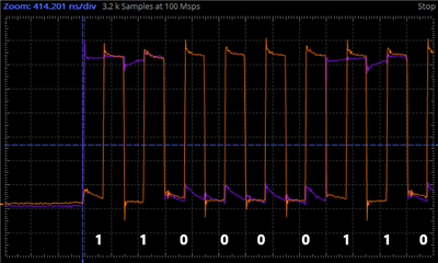
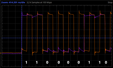
This is all signal for DC=32 and GS=32 to all 32 LED (for two TLC59401). I tried Bit Bang driver instead SPI, but result was same. This problem (MSB force to 0) is not happen in GS data, only on DC data.

If I changed SPI Mode 0 to 3, this problem disappeared. But SPI Mode 3 cause 'SCLK Idle is High', it is different to datasheet.

My LED board has four TLC59401 and 64 LED, I wrote driver software that add 96bit dummy data to top of DC data, it works fine.  

  • Hi,

    Thanks for reaching out!

    Actually, I have received the same problem from another customer recently. Although we haven't verified it yet. But based on your test information and test waveform from another customer. TLC59401 does have this problem.

    Could you please send the DC command twice to avoid this problem?

    BR, Jared

  • Yes, 'Twice DC Data send' can avoid this problem, I tested. It's same as 'send 96bit dummy data before sending DC data'.

    These method will push out corrupt DC data to unused end of SOUT.

  • Hi Susumu,

    Thanks for your feedback,

    I will discuss with our expert and reply you later. Thanks!

    BR, Jared

  • Hi Susumu,

    I suspect that some parasitic capacitance on your interface is causing the signal of your first packet to be distorted and some data is lost. Could you please send some commands that are not relevant to the TLC59401 at the beginning, and then go to send your first command.

    BR, Jared

  • Thanks for your support.

    TLC59401 does not have chip select, so I can't send 'not relevant data'...

    I tried to send dummy SCLK before MODE=1, that means adding dummy GS data, it prevent MSB corruption of DC Data.

    This is oscilloscope wave form of SCLK(orange)  and SOUT(purple) when MSB was OK.

    This is same wave form when MSB was NG.

    This is wave form of SCLK(orange) and SIN(purple) when MSB was OK(with dummy data).

    This is wave form when MSB was NG(with no dummy data).

    I couldn't find difference between OK/NG wave form on SCLK and SIN, but SOUT is differ by with/without dummy data.

  • Hi Susumu,

    Thanks for your quick feedback and such detail waveform.

    The "not relevant data" I mean is the same as "dummy data" you mean. The reason that sending the dummy data first is to avoid the effect of parasitic capacitor. Can I know the waveform is from MCU side or TLC59401 side? And if you add some dummy data first, does the problem still occur?

    BR, Jared

  • I think this problem is caused from output change logic of SOUT.

    I have 4 cascaded TLC59401, so send 63 to 0 value of DC data for 16x4 LEDs. This wave form is leading signals of all 96x4 SCLK/SIN/SOUT of 1st cascaded TLC. So finally latched by XLAT, 1st TLC should have 15 to 0 DC value.

    But 4th TLC will receive 31,62,...,48 DC value, instead of correct value of 63 to 48.

    I suppose that TLC has input shift registers that commonly used on both DC mode and GS mode.

    SOUT is changed from A:Input Shift buffer, B:DC register, C:GS register. In this wave form, SOUT's 15 to 4 value is unnecessary leakage(I think) from DC register that was latched from previous DC data. This A/B/C change logic may be one clock late, and then this trouble will happen, I guessed.

    If you send 63(=0x3f) to DC for all, you will never see this trouble.

    To reappearance of this trouble, I wrote these codes with following steps.

    0.Power on

    1.All register reset

        MODE=1(DC)

        DC=0 to all (96 SCLK x num of TLCs)

        XLAT 1 to 0

        MODE=0(GS)

        GS=0 to all (192 SCLK x num of TLCs) 

        XLAT 1 to 0

    2.Normal data send

        MODE=1(DC)

        DC=32 to all (96 SCLK x num of TLCs)

        XLAT 1 to 0

        MODE=0(GS)

        GS=2048 to all (192 SCLK x num of TLCs)

        XLAT 1 to 0

    3. Start GSCLK(PWM) and BLANK

    In this case, end of LED on cascaded TLCs OUT15 will not turn on.

    To avoid this trouble, these method will effective.

    1. Send DC data twice.

    2. Add some dummy data to top of DC data.  

    3. Send dummy GS data without XLAT before sending DC data.

  • I think SCLK and SIN is same as MCU side waveform. MCU is Raspberry Pi Zero 2, between MCU and TLC, there is TXB0108PW to change voltage 3.3V to 5.0V.

  • This wave form is good pattern with some dummy SCLK.

    DC register leakage is occur in GS data. See following signal.

    I send GS=2048 to 63-48 ( 4th TLC's 16 LEDs). You can see leakage from DC register. But DC data is short, so it will not corrupt MSB of GS data.

  • Hi Susumu,

    Very appreciate for your detail test!

    At first, because this device has been RTM around for a long time, I don't think there should be any problem. So based on my experience, I can tell if the signal distortion is caused by parasitic effects on the interface. However, based on your detailed test results, it is possible that there is a problem with TLC59401.

    The main reason is because we didn't have an EVM board before, so I'm not able to verify it in our office, but I believe your test, Based on the current results, do you still need any help from us?

    BR, Jared

  • On my experiment, minimum method to avoid this problem is:

        after last GS data XLAT or circuit startup,

    "Only one extra SCLK pulse"

        before 96bit SCLK/SIN DC data.

    ”Twice DC data" and "Adding some dummy to top DC data" will work fine, but these are verbose code.

    I don't think our circuit have critical signal distortion from oscilloscope wave form previously shown. This problem occurs 100% in spite of SCLK speed, so parasitic capacitance does not matter. 

    The reason of anyone didn't  notice this problem may be luckily everyone used only all 0x3F DC data or unconsciously sending twice DC data or extra SCLK.

    Don't you think notify for other users is needed for this behavior of TLC and avoidance code if my pointing out was true?


    About 20 years ago, when I was a designer of a VLSI, I have an experience of these kind of logic trouble, that was my mistake, I verified that in real board and Verilog simulation and wrote device driver code for recovering my mistake and release to the VLSI users.

    I recommend to verify this behavior for other TLC users.

  • Hi Susumu,

    Thanks for all the work you work here! I will let other TLC users to know and verify if they have this problem either.

    Thanks very much!

    BR, Jared

  • From TLC5940 sample driver (bit bang) by Aidan Holmes (https://github.com/AidanHolmes/tlc5940),

    there is SCLK 1 to 0 code only first time on reset routine. It can prevent from this behavior.

    def reset(self):

        'Reset pin values'
        GPIO.output(self._blankpin, 1) # set high to disable output (blank)
        GPIO.output(self._progpin, 0) # high to write dot data and low for greyscale
        GPIO.output(self._latchpin, 0) # set high to complete a write to register
        GPIO.output(self._clkpin, 0)
        GPIO.output(self._serialpin, 0)
        self._dotvalues = [0x3F] * 16
        self._greyvalues = [0x0FFF] * 16
        self.write_dot_values() # initialise dot values
        self.write_grey_values() # initialise grey values
        if self._first:
            GPIO.output(self._clkpin, 1)
            GPIO.output(self._clkpin, 0)
            self._first = 0

  • Hi Susumu,

    Thanks for your sharing!

    BR, Jared