This thread has been locked.

If you have a related question, please click the "Ask a related question" button in the top right corner. The newly created question will be automatically linked to this question.

LM5146: WBench power designer output verification

Part Number: LM5146
Other Parts Discussed in Thread: LM5145

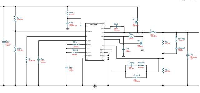
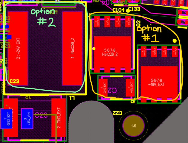
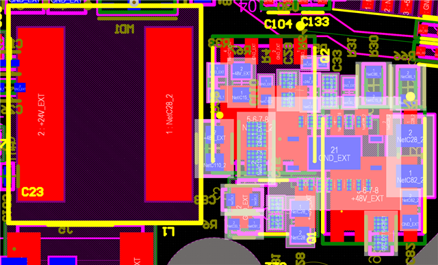
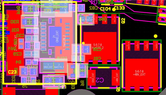
Hello, I used the WBench tool and received the below output in Figure 1. My question is - in the parts list there are qty 2 of M1, are these two parts connected in parallel and the gate of each driven by HO? (See Figure 2 Q1 and Q2)

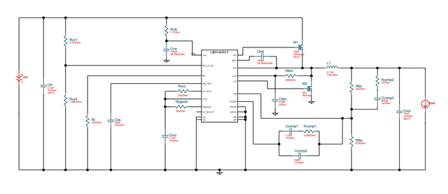
Figure 1: WBench output

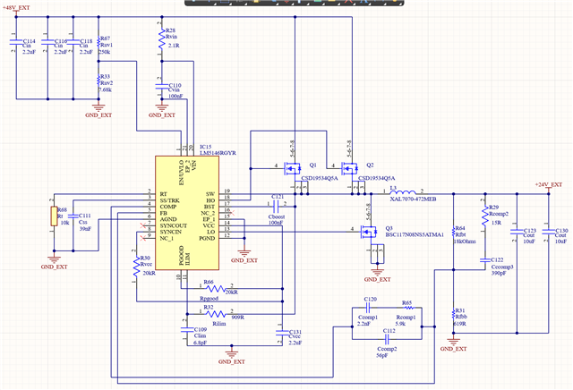
Figure 2: Altium design with WBench output

  • Hi Nicolas,

    Yes, WEBENCH recommended two FETs in parallel based on your specifications (Vin, Vout, Iout, Fsw).

    48V in to 24V out is 50% duty cycle, meaning the high-side FET conducts for half the switching period and has more conduction loss than with the typical step-down ratio of 48V to 12V or 48V to 5V.

    However, the Fsw seems very high here with Rt = 10kΩ, i.e. 1MHz, and two FETs in parallel gives higher switching loss. I recommend using the LM5146 quickstart file to check losses and further improve the design - perhaps using one 80V high-side FET (i.e. you may not need 100V, depending on your Vin-max spec) and moving to a more reasonable Fsw of 400kHz.

    Regards,

    Tim

  • Hi Tim, 

    Thanks for the quick response and resource suggestions. Unfortunately my cloud version of excel is having issues loading the quickstart tool. Instead, I re-ran the WBench tool with the "balanced" option selected instead of "small footprint". This actually gave me a smaller footprint area, one less FET, and a Fsw of 255kHz. This seems like an improvement, please let me know if you have any input to this.

  • Yes, looks much better.

  • Hi Tim,

    Some final questions on this topic...hopefully it is ok to stay in this same thread.

    In regards to the PCB layout, I am trying to replicate the layout found in the LM5146 datasheet but I have less space availability compared to the reference design. I am keeping the in/out bulk caps, FETs, and inductor on the top layer (red). I am putting the LM5146 and its external components on the bottom layer (blue) of the board. I am having trouble deciding what would be the best location underneath the power components to place the LM5146. Below are a couple of options: underneath the FETs, or underneath the inductor.

    Option 1: Underneath FET - Pros: shorter gate drive signal trace, Cons: it is right underneath the main source of noise but based on the reading in the LM5146, the noise should be blocked by the 2 internal ground layers in the board.

    Option 2: Underneath the Inductor - Pros: LM5146 is moved away from noisy FETs, Cons: gate drive traces are longer (~14mm long)

    I am leaning towards Option 1 but would greatly appreciate any input you have. See reference pics below.

    Figure 1: Option 1 and Option 2

    Figure 2: Option 1 with LM5146 and external parts preliminarily placed under FETs

    Figure 3: Option 1 with LM5146 and external parts preliminarily placed under Inductor

  • Hi Nicolas,

    Take a look at the LM5145 EVM, as it's a 2-sided design with controller underneath. The LM5145 is effectively the same controller, just with a reduced Vin-max rating of 75V.

    Regards,

    Tim