This thread has been locked.

If you have a related question, please click the "Ask a related question" button in the top right corner. The newly created question will be automatically linked to this question.

UCC21732: UCC21732

Part Number: UCC21732

Hello,

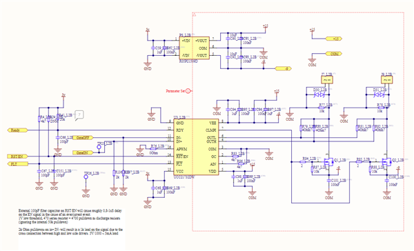
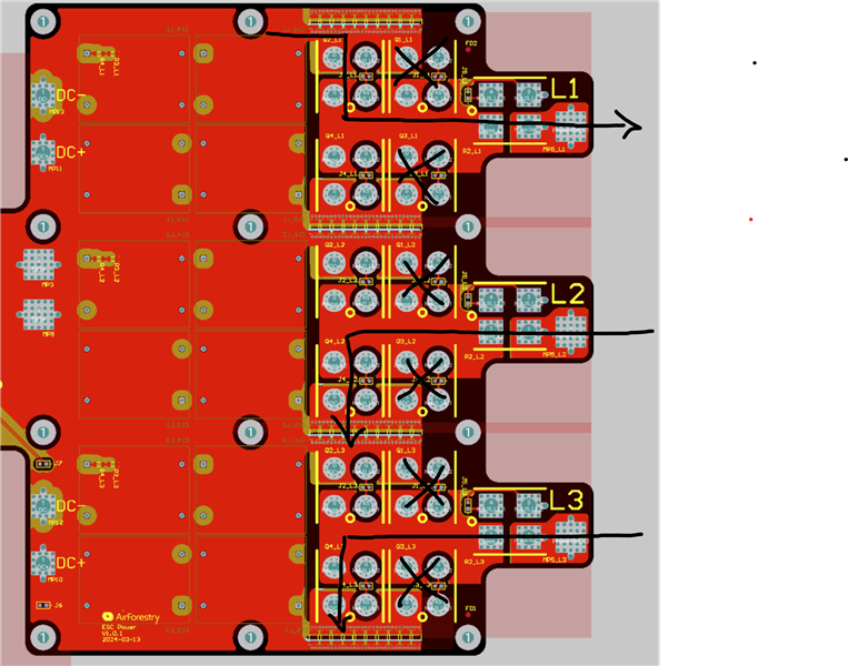
Schematic and a snapshot of the layout is added below.

We are building an inverter using the UCC21732 and having problem with the FLT-pin false triggering. Changes done compared to the schematic below is that the OC-pin and AIN have been disabled by tying them to ground via an 0 Ohm resistors at R83 and R86. Also R76 have been removed so that the APWM is now floating. 

Some conclusions and things we have tried:

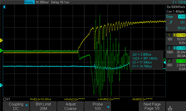
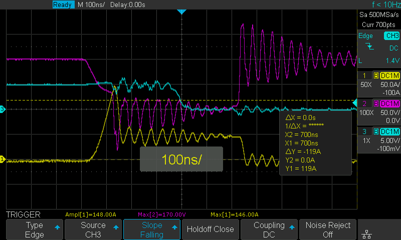
  • It seems to be happening when we increase voltage to around 100V and 150 A. Decreasing the current decreases the FAULT occurence rate. Running at lower voltage more or less removes the issue. We have assumed this is due to the (by us unused) over current pin false triggering.
  • We observed no oscillations on the ready pin.
  • We’re having a single gate driver feeding two parallell mosfets (with separate gate resistors per mosfet) but during testing only a single mosfet is mounted.
  • We’ve tried with 1 ohm gate resistors, 4.7 ohm, and 10 ohm respectively, no luck.
  • It seemed like removing the miller discharge mosfets, Q1 and Q3 decreased the amount of FAULTs.
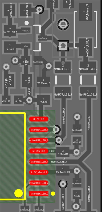
  • The CLMPI pin still had the 2 Ohm and 10k to -9V.

We’ve also tried to replace the UCC21732DW with the UCC21756QDWRQ1 in order to have the desaturation pin instead. With a hope of the higher detection voltage of 5V to solve the problem, but same behavior. 

The main question is why the OC-pin keeps triggering when it's supposed to be deactivated, or is it something we are missing here? 

Best regards, Jimmy

  • Sorry, something went wrong with the added schematic Slight smile

  • Hi Jimmy,

    Is there 4k Ohms between OC and COM? Have you tried making this 0 ohms? Maybe there is enough noise injection at high current to produce a voltage across 4k Ohms at V(OC)?

    Best regards,

    Sean

  • Hi Sean, no we have changed the 4k7 resistor to an 0 Ohm at the OC-pin, the same for the AIN-pin. So this is the big question we can't get our heads around, that the OC-pin can get triggered when tied to COM and is supposed to be deactivated.

    BR, Jimmy

  • Hi Jimmy,

    I hope that there can a simple answer so let me clarify a few things with you before we try and go into the IC design.

    Does the part still work after the fault is cleared? Is there damage to the FET that the fault pin could be correctly reporting upon?

    Do you have oscilloscope measurements for what your switch node ringing looks like? Maybe you are injecting ripple into the gate driver supply through the gate. Damping switch node ringing is sometimes enough to prevent false triggering inside the chip.

    Best regards,

    Sean

  • Hi Sean,

    The FET still works after the fault, we can just reset it and do the test over and over. We also thought that it could be some ringing triggering the FLT-pin, that's also why we switched to the UCC21756QDWRQ1 with the DESAT-pin instead in hope of it being more immune to false triggering, but basically the exact same behavior.

    Below you can see a measurement on the gate. The yellow trace is the voltage over the gate in reference to COM, and the green is current into the gate. Turquoise is phase current. To be noted is that the voltage ringing on the gate can be improved a lot when we manage better probing.

    Some extra details; We use an AC current probe from, "Teledyne T3RC0300-UM"  with BW up to 30MHz and our differential probe is the "Pico TA043" with BW 100MHz.

    BR, Jimmy

  • Hi Jimmy,

    Ringing that depends on "better probing" means that something else is strongly radiating this frequency, which your probe antenna is receiving. Your measurement above does not include the switch node, but maybe your differential probe is high-voltage enough to take this measurement.

    You might need to work on damping an LC resonant switch node frequency that is struck when you close the switch. 

    The simple, inefficient way is to further increase the gate resistor. If you can reduce the dV/dt below the LC resonant frequency, this ringing will not occur. However, this drives up switching losses.

    The other way is to damp the ringing with a high-voltage snubber circuit. That way even if you use a fast dV/dt, the ringing will be damped. You can measure the resonant frequency, and use 1/sqt(LC) = 2pi*f to estimate the L_drain and C_sw that you have. For more precision, you can test the frequency shift with added capacitance, and get 2 equations and 2 unknowns. Then, you can pick a high-power rating resistor to use for snubbing. Since the switch node is shorted to the HV supply, you can put the snubber there to avoid charging and discharging it every cycle. It has to occupy the lowest inductance path to allow the high frequency current to mostly flow from the resistor. 

    This ringing is likely the root cause of the fault, and if we can slow it down, the device should work up to full power.

    Best regards,

    Sean

    5758.GateRing3.TSC

  • Hello, thank you for all the tips. We have measured the switch noise now, see below. We are trying to figure out what our next move should be. Also, can you see that this would also trigger the DESAT-pin on the other IC?

    Turquoise is the FLT-pin

    Yellow is the Drain-Source current

    Purple is the Drains-Source Voltage

    BR, Jimmy

  • Hi Jimmy,

    Nuisance operation is a common issue with protection features, like the DESAT in this device, unfortunately. Most of our new devices have deglitch filters added, which add to the propagation delay, but improve noise immunity. 

    The next step should be to address this LC resonant frequency of the switch node. Can you show more of the layout of your high-voltage current path? High frequency performance is often all about the "plumbing". 

    There are two options that I recommend. One is reducing the length of the high current path from the large decoupling capacitor through the switches and back to the capacitor. This will reduce L and might push your resonant frequency high enough to allow parasitic resistances to begin dampening the resonance.

    The second is to try and damp this resonant frequency. This requires a high power resistor in series with a ceramic capacitor, and this has to be the lowest inductance decoupling path. That way, when the switch closes, it has to draw high frequency current through a resistor, which is then in series with the inductor. You can calibrate this resistor to get the most dampening out of it using the method in my previous post.

    Another option is to keep increasing the gate resistance. This will add losses, but it is commonly done and will slow the dV/dt below the LC resonant frequency of the switch node. Maybe you can try it as a proof of concept. It might be preferable to tighten your layout for the production hardware.

    Best regards,

    Sean 

  • In the picture here you can see the current path for the test we are doing. We can see that it is L2 and L3 that are tripping while we are requesting a step response on L1. Also, this will not happen if we request the step response on L2 or L3. 

    For the gate resistors we have tried 1, 4.7 and 10 Ohm without seeing any real difference. We will try to see if we can figure something out layout-wise.

    BR, Jimmy

  • Hi Jimmy, 

    It's hard for me to visualize where the high-voltage capacitor completes the circuit, and what the high-voltage loop lengths of each phase compare. But it looks like you have room to add local HV bus snubbers with several parallel resistors. 

    I have used the built-in ESR of electrolytic capacitors to solve this problem, but this is often not recommended for long-term reliability.

    Best regards,

    Sean