This thread has been locked.

If you have a related question, please click the "Ask a related question" button in the top right corner. The newly created question will be automatically linked to this question.

TPS562200: Need Support for RE test issue resolution

Part Number: TPS562200
Other Parts Discussed in Thread: TLV62568

Hello,

We need help here to solve RE testing failure issue.

We are doing RE test in one of the project and we are facing RE failure issue since long time and we have tried multiple iterations to solve it but still we do not have that much significant improvements.
Please see below details of our design.
We do have following board structure.
1)  Main Board which has Sigma Star SoC and  - Connected to Camera Board using PVC cable
2) Camera board has Image sensor Sony iMX335  - Connected to Main Board using PVC cable 
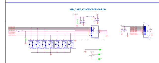
3) we do have separate SD card board - Connected to Main board using Flex cable
4) one is IR LED board - connected to main board using ribbon cable
Camera MCLK is 37 MHz, MIPI is on 594 MHz and SD card frequency is 40 MHz. 
Issue 
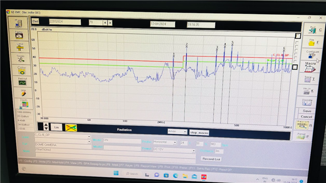
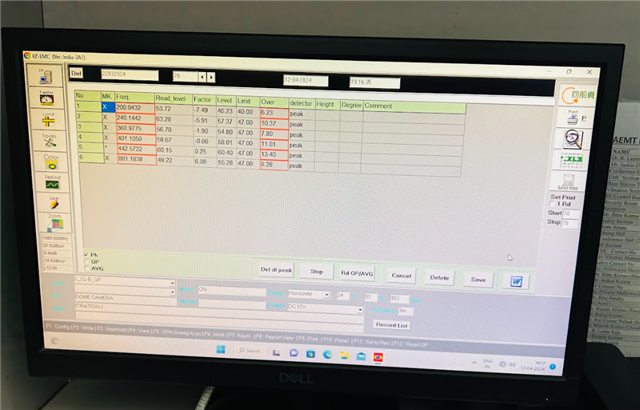
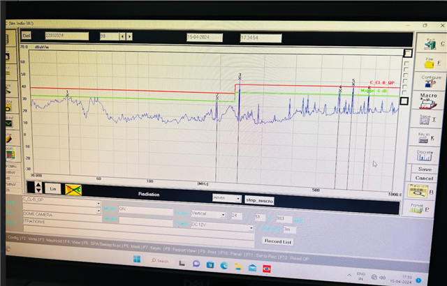
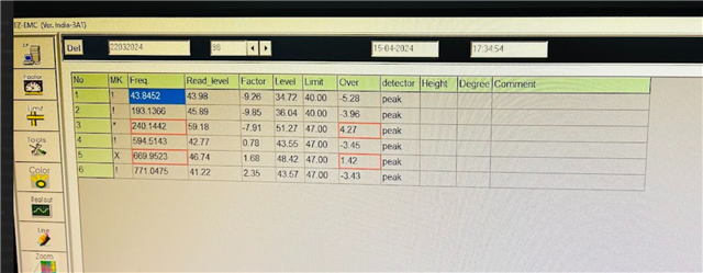
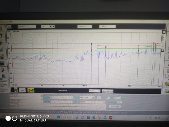
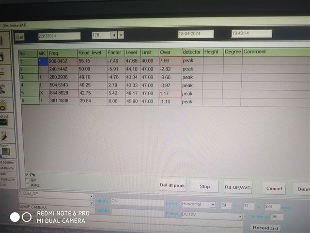
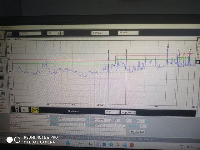
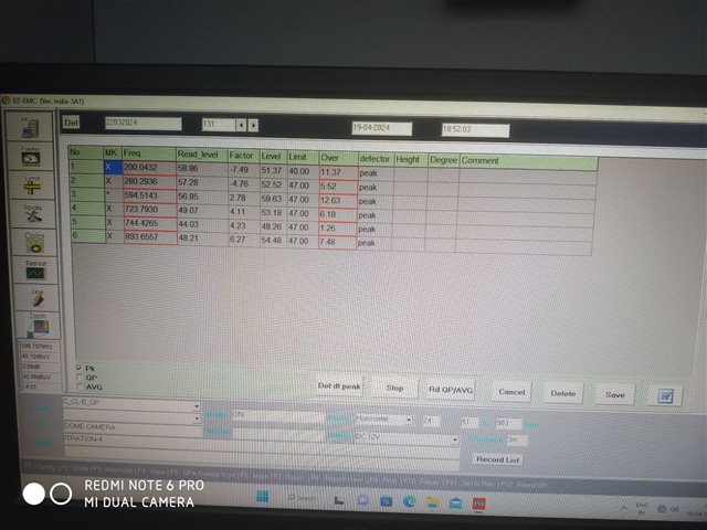
We are having failure on Harmonics of the Camera MCLK and SD card Clock. We have tried with multiple iterations like tuning series resistors of MCLK and SD CLK from 22R to 100R,  reducing drive strength and cable shielding etc but still it does not pass, one observations is when both of them are independently working that time we see that SD is under limit and Camera MCLK goes slighter peak side but issue is when both are running parallel we see major issue.
Till now during all the test iterations we have seen major significant improvements but today (15th APR) we did one test in which seen Good improvement which was done as per below HW modification but still it  is not passing
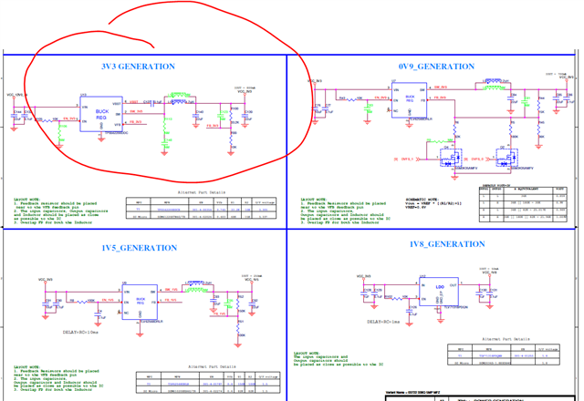
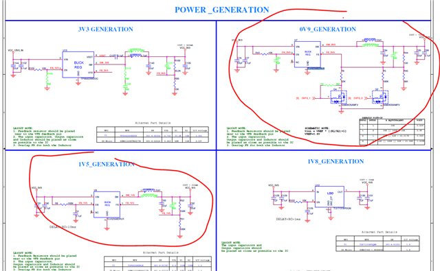
HW modification we did is in Main board : Inductor value changed to 2.2uH & Placed RC snubber ( R= 2E and C = 680pF) on 3.3V regulator (We see Good Improvement with this rework
 
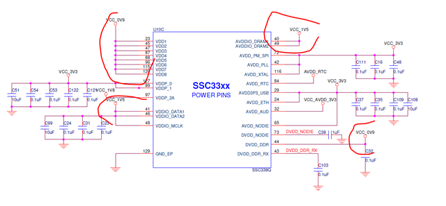
Here we are attaching 3.3V generation design and 3.3V supply provided  to peripherals. Current drawn on 3.3V is approx 800mA
Also attached RE test results before 3.3V output HW modifications and after 3.3V output HW modification
Please suggest how this HW modifications helped us and what can be done further on supply side if we do have to get still best result and have to pass RE test.
  • Please see attached docs.

    3.3V Generation                 Camera Supply                        uSD card board


    Before 3.3V Ouput HW modifications


    After 3.3V output HW modifications


  • Hi Brijesh,

    Have you try changing the RC snubber value? You can measure the SW node voltage and adjust the Rsnub and Csnub to get a lowest SW spike. And the inductor direction can also affect RE. You can try to rotate the inductor8 to see if any improvement.

    Best Regards,

    Shipeng

  • Hi Shipeng,

    We have measured SW node Voltage and calculated RC snubber values from calculation we are getting R=4E and C=0.2uF so we have used this values and tested again. we see little bit good improvements but still it is not passing. We checked inductor polarity as well so there is no polarity in the inductor we have used.

    Please see results with R=4E and C=0.2uF snubber values and suggest us better way to pass RE. We are really stuck and need to solve this issue in a very hard time limit.

  • Hi Brijesh,

    Sorry I don't know R=4E refer to? Do you mean 4Ohm?

    Could you measure the SW waveform by a 500MHz or higher probe/oscilloscope to see if it produces these frequency's noise? 

    Another thing you can try is adding a 5Ohm resistor in series with C127.

    Thanks.

    Regards,

    Shipeng

  • Hi Shipeng,

    Yes 4E means 4 ohm resistor.

    Could you measure the SW waveform by a 500MHz or higher probe/oscilloscope to see if it produces these frequency's noise? - Yes will try.

    Another thing you can try is adding a 5Ohm resistor in series with C127 - How this will help?

    Thanks,

    Brijesh K

  • Hi Brijesh,

    Adding the resistor can slow down the slew rate of SW voltage and reduce the spike.

    Thanks,

    Shipeng

  • Hi Shipeng,

    We can try that but will it cause any problems? Like switching  regulators efficiency can be down and start up issue or any performance issue will it cause? 
    Should we Keep Snubber RC values 4R and 0.2uF with this 5R series resistor rework? 
    Thanks,
    Brijesh K
  • Hi Shipeng,

    Waiting for reply please as we do have to go RE LAB for testing so can u plz confirm above so can rework it and go for testing?

  • HI Brijesh,

    Adding resistor can improve a little power loss, no other problems. RC snubber don't need to be changed.

    Thanks.

    Regards,

    Shipeng

  • Hi Shipeng,

    Thank you for suggestions and confirmation, will try this and let you know results.

    Thank you,

    Brijesh K

  • Hi Shipeng,

    This are results with Adding Series resistor 5.76 ohm with C127, Snubber is R = 4 ohm & C = 0.2uF. Results seems not good. Please suggest better way.

  • Hi Shipeng,

    Waiting for your valuable suggestion please. 

    Thanks

    Brijesh K

  • Hi Shipeng,

    Except 3.3V we do have other 2 regualtors as well in our design.

    1) 0.9V regulator (SoC) Core supply -  700 mA  and 2) 1.5V regulator - (SoC and Internal DRAM) - 250 mA


    Do you think that these both also can be source of Radiations Because we have seen improvements by pacing RC snubber on 3.3V regulator so do you have any thoughts for these other 2 regulators?

    Thanks,

    Brijesh K

  • Hi Brijesh,

    Yes, all swithing regulators can be source of EMI so you can add RC snubber circuit to them. You can also post a new e2e thread to get advice from TLV62568 engineers.

    Thanks.

    Regards,

    Shipeng