This thread has been locked.

If you have a related question, please click the "Ask a related question" button in the top right corner. The newly created question will be automatically linked to this question.

BQ28Z610-R1: ESD protect on I2C bus.

Part Number: BQ28Z610-R1
Other Parts Discussed in Thread: EV2400, BQ28Z610

Hi everyone.

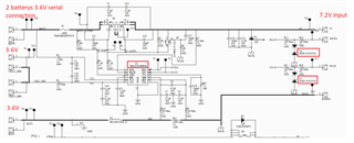
I have a design use  BQ28Z610-R1 as attached file. I also use  ESD5581N2T5G to protect I/O pin when I connect them with external peripheral device.

I have tested this PCBA FCT(Programming with EV2400), they are working without any problem, but when we apply weld process after that we test this PCBA FCT(Programming with EV2400) again we can not program or scan I2C address on my PCBA (ratio 5% in my production), that means I2C module of  BQ28Z610-R1 have a problem after weld process. I replace the new BQ28Z610-R1-> this PCBA passed. I Use battery 7.2V and power supply for Pack pin is 7.2V.

I know that:

        - ESD5581N2T5G have Voltage Reverse:5V, Voltage clamping 12V.

        - BQ28Z610-R1: SDA, SCL Pin input maximum 5.5V as datasheet mentioned.

My concern:

       - Whether when we apply weld process, it will generate ESD, this ESD can damage 2C module of  BQ28Z610-R1. But I have ESD diode to protect this, so why this can happen?

      - SDA, SCL Pin input maximum 5.5V as datasheet mentioned, we use ESD diode with Voltage Reverse:5V, Voltage clamping 12V. This diode can protect 2C module of  BQ28Z610-R1 or not?

      - If we change ESD5581N2T5G to an ESD diode with Voltage Reverse:3.3V whether we can improve this problem.

      - Do you have any advice to improve my situation?

  • Hi Anh,

    In regards to ESD, it is typically difficult to pin down the root cause of where this is occurring. Will looking at the schematic you have sent, we would recommend adding spark gaps to both the SDA and SCL lines of the device, along with the PACK connection. This can also be seen in our bq28z610EVM schematic:


    https://www.ti.com/lit/pdf/sluube3 

    More ESD mitigation techniques can also be found in Section 10 of the bq28z610 datasheet below:

    https://www.ti.com/lit/gpn/bq28z610 

  • Hi Anthony.

    Thanks for your respond.

    Could you please help me to explain more about "adding spark gaps to both the SDA and SCL lines of the device". That means in the layout we must have an empty space between the SDA and SCL line, that's right?

  • Hi Anh,

    You are correct, a spark gap in essence is a line going to ground connected to the SDA and SCL lines of the device, however when designing them, the space of the gap is very important. In the design above for the bq28z610, we use the spacing below:

    Regards,

    Anthony Baldino