Hello,
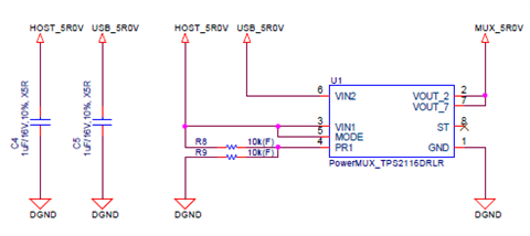
In the circuit below, I switch between the 5V input of VIN1 and the USB VBUS of VIN2.
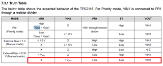
The operating mode is priority mode.
I am currently experiencing the following symptoms.
1. When VIN1=5V input and VIN2=floating, the same voltage as VOUT appears at VIN2.
At this time, the 5V current of VIN1 is 1A.
2. Next, when VIN1=5V input, VIN2=USB VBUS 5Vinput, the current consumption of VIN2 USB VBUS is 300mA, and the current consumption of VIN1 5V drops to 700mA.
The total current consumption of VIN1+VIN2 is 1A, which is the same as 1. It appears that both VIN1 and VIN2 are output to VOUT.
I suspect that the internal FFT of the TPS2116 may be short.
What could be the cause of TPS2116 causing these symptoms?
The 5V input of VIN1 and VIN2 are both tyv 5.0V, and the voltage exceeding the absolute maximum rating of 6V is not applied.
Best Regards,
Hiroyuki Taguchi