Other Parts Discussed in Thread: , TPS2376
I have a working design for TPS2375 for POE functionality. And I had to do a new version of this design, adding some additional functionalities, headers ..etc. And I in the first prototypes the POE voltage does not build up. The operational mode does not reach PD powered mode. Which is strange, because this design was working before and I did not changed the layout and components on the board. Using same MPN devices, same board stack-up.
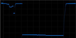
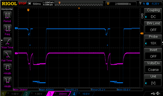
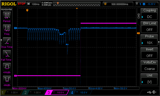
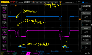
Measuring the GND(RTN)-VSS I got this measurement on scope (negative voltage because the reference is GND):
It seems the detection, classification finishes, ~53V appears, but it could not manage to go into the PD powered mode state. Does anybody see any strange thing on this measurement?
On GND-VDD I did not notice anything. Seems like the RTN never switches and so it is floating.
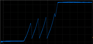
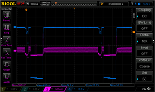
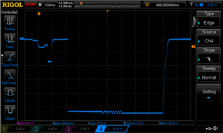
On the working device (previous version of the board) I have this on GND-VDD:
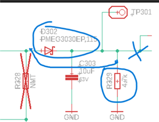
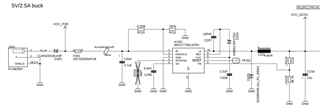
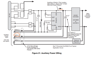
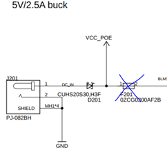
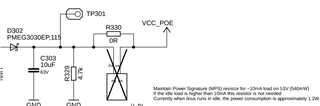
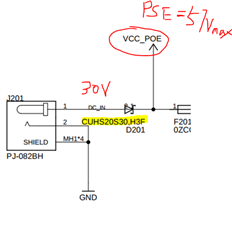
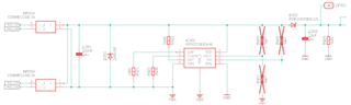
Related schematic:
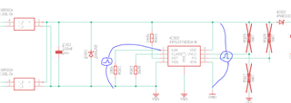
And layout:
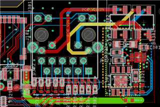
The footprint and circuit is prepared for TPS237x devices as well.
What can be the issue here?