This thread has been locked.

If you have a related question, please click the "Ask a related question" button in the top right corner. The newly created question will be automatically linked to this question.

UCC21732-Q1: GD_FLT false tripping

Part Number: UCC21732-Q1
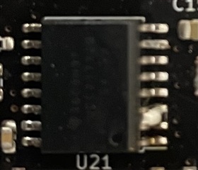
Other Parts Discussed in Thread: UCC21732

Hello, 

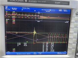
It seems like I'm getting unexpected GD_FLT tripping. I'm using this in a synchronous buck converter, and I have two phases interleaved (4 UCC21732 devices GD_FLT output connected together). I'm operating in open-loop with a fixed duty cycle, and as I increase the voltage, I get a GD_FLT. I have the OC pin directly shorted to the COM pin here. 

It seems like this issues might be correlated to peak inductor current because if I double the switching frequency, I can achieve double to bus voltage. Additionally, I can operate well past the tripping voltage if I disconnect my inductor and just turn the devices on/off (no reactive current flow). 

GD_FLT is CH1 (yellow)

  • Hi Jimmy Palmer,

    Thanks for sharing your observations and capturing the waveforms during the failure. 

    1. is the OC short to COM close to the device pin?

    2. Is it possible to share your system details in terms of "block diagram"? I am curious to see the position of the gate driver board to the inductor and how it is connected.

    3. In your statement "It seems like this issues might be correlated to peak inductor current because if I double the switching frequency, I can achieve double to bus voltage." -  does it mean that you observed this issue when the load current is increased. (at what value failure is observed?)  and also at what voltage? When you disconnect the inductor, no failures observed , even for increased voltage - is the assumption right?

    4. what is the tripping voltage in your system?

    5. In the waveform what you shared, I see PhA, PhB current, FLT (combined for both phases???), VSWA  (switch node voltage?) - is our understanding right? 

    Based on the description, it is possible that the noise in the system causes the failure, I can see FLT is very noisy in the capture.

    Looking forward for your inputs, to effectively debug this failure scenario.

    Thanks

    Sasi

  • 1. is the OC short to COM close to the device pin?

    Yes. I soldered the pin directly to COM. 

    2. Is it possible to share your system details in terms of "block diagram"? I am curious to see the position of the gate driver board to the inductor and how it is connected.

    Sure thing. I will work on a block diagram of the setup. 

    3. In your statement "It seems like this issues might be correlated to peak inductor current because if I double the switching frequency, I can achieve double to bus voltage." -  does it mean that you observed this issue when the load current is increased. (at what value failure is observed?)  and also at what voltage? - I have no load right now. All of the energy is reactive between the inductor and output capacitor. Here's a summary of fault points:

    50kHz - 150V 

    100kHz - 300V

    200kHz - ~450 to 500V

    -When you disconnect the inductor, no failures observed , even for increased voltage - is the assumption right? - yes, no failures.

    4. what is the tripping voltage in your system?

    I don't have any overvoltage protection implemented. This is just running in open loop with only the desat protection active. 

    5.  In the waveform what you shared, I see PhA, PhB current, FLT (combined for both phases???), VSWA  (switch node voltage?) - is our understanding right? 

    Yes the the FAULT signals are all tied together. 

    UPDATE: 

    I increased the gate resistance for all of my devices from 1.5R to 3.3R. It seems there is a little more buffer now. I can operate with 100kHz, 300V now, but at ~325V the FAULT signal trips and goes low. 

  • Hi Jimmy,

    Thanks for the detailed response. I will look forward for your system block diagram image.

    Good to hear that increasing gate resistance improves the fault failure signature.

    I thought that the inductor is "actual load", simulating the motor condition. but in your response,  you have mentioned that there is no load - how is the inductor planned?

    I believe that your system block diagram image will help to understand the system better. Looking forward for your inputs.

    Also interested to know what is the expected max functional power level of your system.  (voltage and current)

    Thanks

    Sasi