

Tool/software:
Benefits of UCC5880 over UCC587x

This thread has been locked.
If you have a related question, please click the "Ask a related question" button in the top right corner. The newly created question will be automatically linked to this question.
The UCC5880-Q1 device is an isolated, highly configurable adjustable slew rate gate driver. One element that makes UCC5880 very useful in high power EV/HEV applications is it’s SPI based device configurability, verification, and diagnostics.
Although the SPI communication provides a lot of flexibility for the system, some applications do not require the complexity of SPI. Customers who are not familiar with SPI may appreciate its benefits, but when getting started with this new driver, may want to do a simple evaluation without spending time and resources developing the software. The UCC5880-Q1 device can support this as it can be used without SPI communication for initial evaluation of the device
Using this functionality, the engineer can evaluate basic driver performance like drive strength, switching losses with power modules, adjustable gate drive, short circuit protection, etc. The user will be able to speed up the evaluation process since there is no requirement to develop any new code or even connect to a computer.
|
Features |
UCC587x |
UCC5880 |
UCC588x benefits |
|
Functional Safety |
FS compliant (ISO26262) |
FS compliant (ISO26262) |
|
|
Pin count/ Pkg body |
36 DWJ (0.65mm pitch) (7.5x12.8mm) |
32 pin DFC (7.5x10.3mm) |
Smaller package increases power density |
|
Drive current |
15A (typ) |
15A+5A Dual O/P (typ) |
Split Dual output structure for slew rate control |
|
Desat/ OC /SC |
Y/Y/Y |
Desat or OC/SC |
Increased protection features for GDIC and system levels |
|
ASC |
Y (primary & secondary) |
Y (primary & secondary) |
|
|
Fault monitoring |
Y (extensive) |
Y (extensive) |
|
|
VCE clamp and Gate Monitor |
Y |
Y |
|
|
Gate threshold monitor (Store in MCU) |
Y |
Y |
|
|
TSD, OTW, OV monitors |
Y |
Y |
|
|
SPI interface |
Y |
Y |
Increased configurable register settings |
|
Programmable Settings |
Y |
Y |
|
|
Integrated diagnostics, BIST |
Y |
Y |
|
|
Real-time Variable Drive Strength (SPI & Pin selectable) |
N |
Y (3 levels on the fly) |
Balance switching losses vs VDS overshoot |
|
Integrated ADC |
10Bit-6 ch external, die temp |
10Bit-2 ch external, die temp, DESAT, VCC2 |
Increased ADC configurability and accuracy |
|
Miller Clamp |
Y (Internal and External) |
Y (Internal and External) |
|
|
Isolation |
Reinforced(5.7kV) |
Reinforced (5.7kV) |
Increased transient immunity |
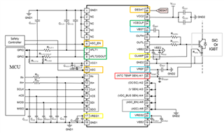
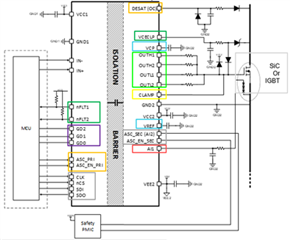
UCC587x Application Diagram UCC5880 Application Diagram
The UCC5880 has improved upon the previous UCC587x by optimizing the pinout/supply topology allowing lower pin count and a smaller package to 32 pin DFC package vs the 36 pin DWJ, achieving better performance and power density. Below is a table depicting the differences and similarities in the pinout and functionality of the devices.
UCC588x Pin/feature change vs UCC587x
|
Pin Function |
Connection change |
Reason for Change |
|
Primary Side |
||
|
ASC primary |
Same connection |
N/A |
|
nFLT1/2 & Dout |
Same connection |
N/A |
|
VREG1 |
Different Connection |
Simplify Design and remove noise coupling path |
|
SPI pins |
Same Connection |
N/A |
|
GDx pins |
New Pins |
Added external control for drive strength selection |
|
Secondary Side |
||
|
DESAT |
Desat and OC pins combined |
Simplify Design |
|
VCECLP |
Same connection |
N/A |
|
VBST/VREF |
Same connection |
N/A |
|
CLAMP |
Same connection |
N/A |
|
ASC Secondary |
Same connection |
N/A |
|
VREG2 |
Different Connection |
Simplify Design and remove noise coupling path |
|
OUTPUT |
Different Connection |
Dual Split output structure for adjustable drive feature |
|
Analog Inputs |
Different Connection |
Reduced number of redundant analog input pins |
UCC5880 adds the variable gate drive feature with its new innovative output structure. UCC5880 has a dual-split output structure compared to a simple split output structure of UCC587x. This then gives the device the ability to use 3 different combinations for turn on and turn off. The driver can also switch between the different drive strengths on the fly using SPI commands or an external control with the GDx pins. This gives the user the ability to control the drive strength for different load conditions, ultimately leading to significant improvements to efficiency and EMC. Based on TI’s inverter testing, Adjustable Gate Drive gives an increased 2% efficiency gain.
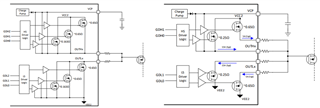
UCC587x vs UCC5880 Output Stage Diagram
UCC5880 enhances SPI communication requirements to increase flexibility and configurability to the SPI programming of the device.
Key changes to UCC5880:
UCC5880 adds continuous mode sampling to allow digitization without PWM toggle for easier start-up diagnostics. ADC channel bits can be used to include measurements in round robin when PWM is static high or low. VCC2 and DESAT nodes have also been added to the MUX and can be measured and reported in the ADC register.
UCC5880 also boasts increased ADC configurability and accuracy. The table below shows the total unadjusted error based on the improved datasheet specifications.
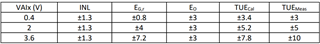
UCC5880 ADC Accuracy Results
In a typical inverter system, noise can couple into the device through Switch node noise, ground loops, noise from other systems, hole in shield walls, DC bus bars, etc. Therefore, it is important to choose a robust and reliable gate driver. UCC5880 has significant improvements over UCC587x in regards to robustness.
Key Lane Improvements:
A major improvement of UCC5880 over UCC587x is the ability for UCC5880 to drive the power stage without the need for SPI control or communication. This prevents the user from needing to design any software for simple evaluation of the driver for Double Pulse, which directly results in a shorter development cycle time. To learn more about using UCC5880 without SPI, please see the FAQ here.
UCC5880 adds a new 16- bit SPITEST register which may be written with any data pattern. The read back of these contents can be used to test SPI engine health during diagnostics cycles and SPI test routines from the controller.
