This thread has been locked.

If you have a related question, please click the "Ask a related question" button in the top right corner. The newly created question will be automatically linked to this question.

UCC14140-Q1: Output noise is detected even no load is applied.

Part Number: UCC14140-Q1
Other Parts Discussed in Thread: UCC14141EVM-068, UCC14141-Q1

Tool/software:

Dear TI experts,

My customer now tests UCC14140-Q1 in their own PCB.

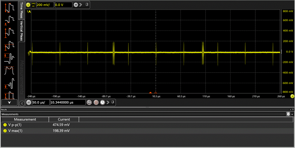
They fould that there is ripple noise in the 15V output even no load is applied.

I attach the waveform of AC noise and DC noise.

1. AC noise

2. DC noise

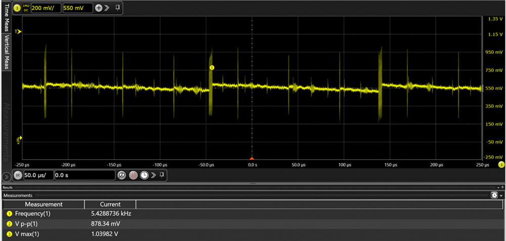
I also attach the schematic and layout for your convenience. (they measured AC and DC noises on 15V output.)

Power Switch (002).pptx

Please review this issue, and advise me about reducing this noises.

Best regards,

Chase

  • Chase,

    From section 5.5 of the UCC14141EVM-068 User Guide here, you can see what the AC ripple voltage waveforms should look like and from section 9.5 of the UCC14141-Q1 data sheet here, you can see follow the recommended PCB layout guidelines.

    1. Only one single via is used to at C36 compared to several vias shown on the EVM. this is the path for VDD-VEE bias power deliver to pin 6 isolated gate driver. Follow guidance from the EVM and add more vias.
    2. No 330pF capacitor is used for HF noise bypass across R3. Please add 330pF parallel with R3 and closest to U2.
    3. No VCC bulk capacitance is used at U1, pin 6-4. Suggest better placement of C6 as HF bypass capacitor for gate driver and add some bulk capacitance (1uF-4.7uF typical) in parallel with C6.
    4. Gate drive path from R10 to Q2 is long and no GND plane is used. Also, the gate drive track passes parallel to top layer GND plane shred between U1 and U2. The HF noise seen in your attached scope plots might be a result of gate drive coupling switching noise into the GND plane. Please measure the gate drive signal and the UCC14141 output ripple on the same plot to confirm?
      1. Consider to place the gate driver as close as possible to the SiC
      2. Please add shielding GND layers by using the internal PCB layers as GND
    5. No thermal vias are used. Please add thermal vias as shown in the PCB design recommendations in the data sheet
    6. Make sure to use X7R or better capacitor dielectric and at least 2x voltage rating if possible.

    Regards,

    Steve