TPS650330-Q1: no output voltage issue

Part Number: TPS650330-Q1

Tool/software:

Hi, Support Team

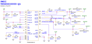
our client first time use TPS65033000-Q1, input Vin=12V but no output voltage(+3V3/+1V8/+1V2/V1P8)

how to confirm IC is work?

 schematic as below chart:

also we find TPS6503xx-Q1 Camera PMIC Programming Guide:

https://www.ti.com/lit/an/slvafa4/slvafa4.pdf?ts=1718765418804&ref_url=https%253A%252F%252Fwww.ti.com%252Fsitesearch%252Fen-us%252Fdocs%252Funiversalsearch.tsp%253FlangPref%253Den-US

about 2.3 Default Register Settings
The TPS65033000-Q1 is tailored to program in mass production. The following features help enable this:
• Only the VSYS/VSYS_S/PVIN_B1 input voltage and I2C pull-up voltage are required to communicate with
the device through I2C.
• The SEQ pin must be logic HIGH to enable all regulators.
• The GPIO pin must be logic HIGH to enable Buck3 and the LDO.
This definition enables various paths to production programming as discussed in detail in the following sections.
1. Production line programming
2. Serializer-Deserializer (SerDes) back-channel programming
For a high level overview of the TPS65033000-Q1 default voltage, sequence, and other settings, see the
Camera PMIC Spin Selection Guide.

its mean SEQ pin and GPIO pin default should be pull high and than start up output voltage?

if yes, how to Production line programming  do not use SEQ and GPIO pin?

if any suggestion, Please advise me.

Thanks,

Best regards,

Lawrence

  • Hello Support Team:

       This is TI FAE Roy support the customer with Lawrence. 

    customer  has design TPS65033000-Q1 as Lawrence attached schematic , the both SEQ and GPIO pin floating not connect to VREG pin but they have using I2C connect to MCU.

    I saw PMIC programming guideline can support I2C programming with SEQ pin floating in the Figure 3-2. Reprogramming the TPS65033000-Q1 with an External I2C Controller diagram.

    So can I use the following setting flow to support SEQ/GPIO pin floating from customer design with this part? 

    Step 1 , power on PMIC then Unlock control register  -> Write PMIC ,0x02 ,0xDD

    Step 2 , Write all Buck1/2/3/LDO register  Dh , Eh , Fh , 10h bit 0 and bit 5 to "1"  as “ Not included as part of the power ON/OFF sequence logic”

    Step 3 , Write Register to EEPROM -> Write PMIC,0x4A,0x2D

    Step 4, Power on /off recycle 

    Thank you 

    Roy

  • Anyone can suggest?

  • Hi Lawrence, Roy,

      I'm sorry for the late response!

      Please also insert the step below after step1:  Unlocks the Configuration Registers -> Write PMIC ,0x05, 0xAA.

    Thanks!

    Phil