This thread has been locked.

If you have a related question, please click the "Ask a related question" button in the top right corner. The newly created question will be automatically linked to this question.

UCC27301A-Q1: Request for Guidance on 3KW BLDC Controller Board Design

Part Number: UCC27301A-Q1

Tool/software:

Dear Team,

I hope this message finds you well!

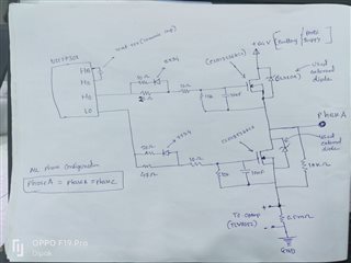
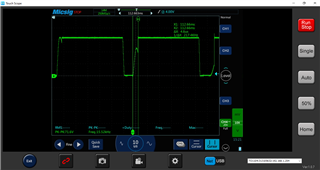
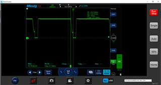
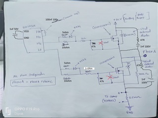
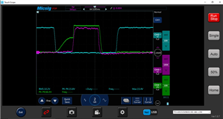
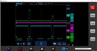
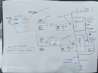
We are currently working on the design of a 3KW BLDC controller board and have implemented the UCC27301 gate driver along with the CSD19536CKS MOSFET. However, we are encountering some challenges related to the MOSFET’s rising and falling edges.

I have attached the configuration details for our gate driver as well as an image showing the MOSFET ringing.

We would greatly appreciate it if you could review the attached schematic and waveform and provide us with guidance on how to resolve these issues.

Additionally, we have observed that when the duty cycle is set to full (running at 15.6kHz), the gate driver output drops to zero instead of reaching the maximum value.

Any insights on this matter would also be very helpful.

Thank you very much for your assistance.

Best regards, 

Dipak

  • Hey Dipak,

    Thank you for reaching out to TI with your question regarding the UCC27301A-Q1.

    Looking at your schematic, the bootstrap capacitor is much larger than expected for HB-HS. Please take a look at the following application note for sizing of that as well as the VDD bypass capacitor that. What size capacitor do you have on VDD?

    Bootstrap Circuitry Selection for Half-Bridge Configurations

    For controlling rise/fall times, adjusting the gate resistors and making them smaller will decrease your rise and fall times. The values that you have selected are larger than typical.

    Have you tried running this without the 10nF Vgs capacitor? This is increasing the effective gate charge requiring greater gate driver to turn on the FETs.

    If you are trying to run 100% duty cycle, you will need to make provisions for biasing the high-side as the bootstrap capacitor cannot support 100% duty cycle. For that, please check out the following FAQ for high-side biasing options.

    [FAQ] How to bias the high side of a half-bridge gate driver and why

    Let me know if you have any questions.

    Thank you,

    William Moore

  • Dear William Morre,

    Thanks for the reply!!

    After your suggestion we made following changes as shown in schematic and we got results as shown below.

    Still phase voltage is not proper as well as high side MOSFET signal.

    Could you please elaborate what is the reason behind phase voltage [ green channel ] is become high even when high side MOSFET is not turned on [ pink channel ]  

      high side is not on but phase voltage is on why?

    Please note:

    - Green channel is phase voltage

    - Pink is high side MOSFET gate to source signal [ measure using differential probe ]

    - Blue is low side MOSFET gate to source signal  

    - Also please have a look at the our snubber circuit as we shown in schematic.

    Best and regards,

    Dipak

  • Hey Dipak,

    Can you share what the output is connected to the switch node (HS)?

    What it appears to be is if HS is not connected to an output and is left floating, during the deadtime, it will float up until HO rising edge occurs.

    Let me know if you have any questions.

    Thank you,

    William Moore

  • Hi William Morre,

    Currently I have connected 1.2kW sensored BLDC HUB motor to the phases.[ phaseA-B-C]

    -Dipak

  • Hi William,

    Sorry we forgot to mention here we have updated our drawing please have a look it.

    -Dipak

  • Hi Dipak,

    Our expert William is currently Out of Office and will be back next week. Please expect a reply before end of next week. Appreciate your patience and understanding.

    Best,

    Pratik

  • Hey Dipak,

    Apologies for the delay due to me being out of office.

    I am assuming that the HS pin was always connected to the switch node of the half-bridge with your updated drawing above.

    During the deadtime between HO and LO, the status of HS is dependent on the power train that is connected to the half-bridge. With the BLDC motor that you have connected to this switch node, there are many factors such as back emf and motor transients that could cause HS to not follow the HO waveform explicitly.

    Looking at the below image, HS is operating as intended during HO on or LO on and the rising edge prior to the HO rising edge is just HS floating up due to the power train.

    I do not see concerns in this as this does not create a shoot through condition.

    Let me know if there are any further questions.

    Thank you,

    William Moore