


Tool/software:
Hello,
I encounter a very big output ripple voltage on the output.
When I use FPWM mode it is very different, The riplle is very low compared to in PFM mode.
I included 2 scope pictures of the output voltage. Both are 12V/100 mA
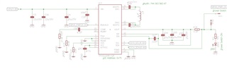
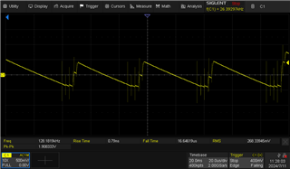
Above in PFM mode
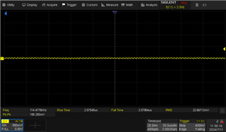
In FPWM mode
But the proble is that the efficiency is ver, very low in this mode. With no load, the circuit is consuming approx 60 mA.
In PFM mode, without load it consumes only a few ma's
With a maximum powerload of 200 mA, I preffer PFM mode.
Why is there so much ripple? adding capacity to the output don't seem to help.


