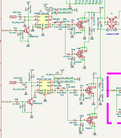
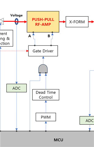
UCC27614: Abnormal work in gate driver.

Part Number: UCC27614

Tool/software:

Dear master.

I'm using UCC27614   8pin SON DSG Package.

■ UCC27614 Operating Condition.

   - Operating Freq. : 500kHz / 300kHz.

   - FET : BSC146N10LS5 parallel driving.

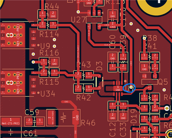
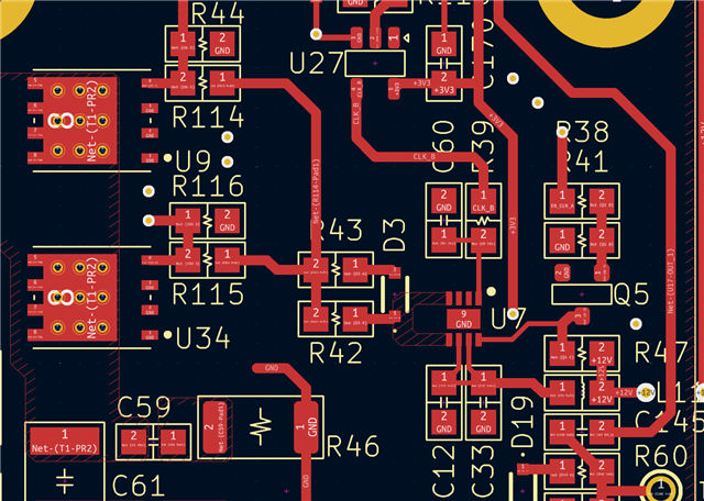
   - Schematic & pattern : See below.

   - 1.6T 2 layer PCB.

-Trouble : 1 PCB is  out of order. 

                 1 PCB has operating abnormal operation.

Can you advise to me what's wrong?
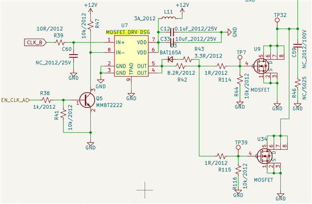
                 

Schematic

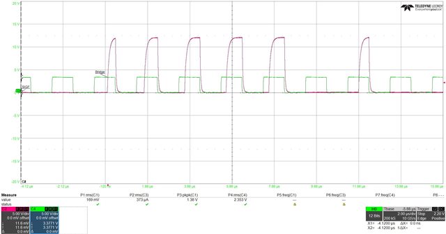
Waveform

Copper PatternPatternThermal Image

IC Marking

  • Hi Sanghyun,

    Thanks for reaching out to TI.

    Overall, the schematic looks mostly okay, but I do have some follow-up questions:

    1. Can you comment on the L11 inductor on the VDD pin connected to pin 6 and 7?
    2. Can you confirm the timing on Clock_A and Clock_B and if they are synced?
    3. Can you send an updated waveforms diagram that contains the following:
      1. IN+
      2. IN-
      3. VDD
      4. OUTPUT

    Thank you!

    Jeremiah

  • Dear Jememiah.

    Thanks for your fast response.

    1)  L11 : MH2029-800Y

    www.mouser.kr/.../mh-777565.pdf

     2) CLK_A, CLK_B is Pushpull type RF-AMP.


    3) CLK_A, CLK_B, EN_CLK_A  signal is controlled by MCU.

      -First.  VDD(+12V) is always on when system turn on.

      - Second. CLK_B is on when user start.

      - Last. EN_CLK_B is HIGH.

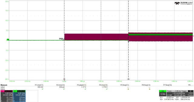
    Please see below waveform. 

    ※ C2(Magenta) : CLK

        C4(Green) : Enable.


  • Hi Sanghyun,

    Thanks for your patience over the weekend.

    Taking a second look, there may be a chance the output waveforms are affected by the EN-CLK-A going low, shutting of the output. However, I'd like some more clarification on some points (my apologies for not specific enough requests!):

    1. What the use case is for the L11 inductor on the VDD pin?
    2. Are the Clock_A and EN_CLK_A synced?
    3. Can you send an updated waveforms diagram that contains all the following in one diagram, with a 2us/div (the previous response only has CLK and Enable on a 1ms/div)  :
      1. IN+
      2. IN-
      3. VDD
      4. OUTPUT

    Thanks!

    Jeremiah