Tool/software:
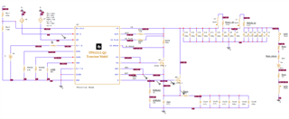
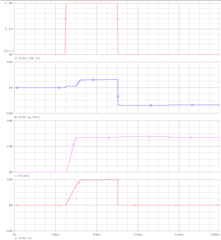
I was implementing inrush current control feature of TPS12111 by using INP_G and G pin as described in datasheet.
According to datasheet during this operation when the INP_G signal is Low, G voltage pulled low to SRC. But during my simulation
I have observed it is getting pulled to GND. Because of this MOSFET (M2) is getting negative voltage across VGS pin. Could you please go through
the schematic and waver forms shown below and clarify this issue?