This thread has been locked.
If you have a related question, please click the "Ask a related question" button in the top right corner. The newly created question will be automatically linked to this question.
Tool/software:
Hello,
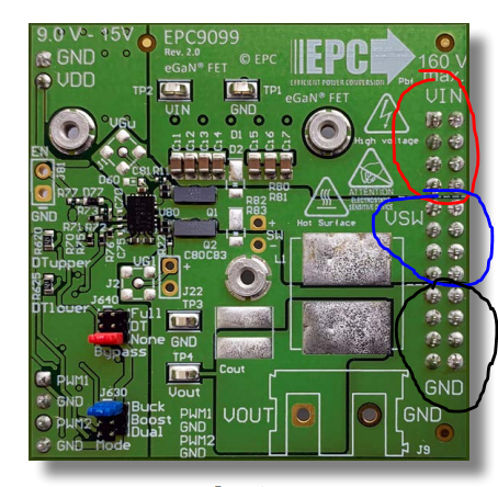
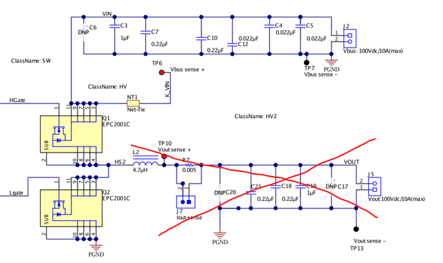
I am using LMG1210 gate driver ICs to drive a Full H-Bridge. I'm interested in using the LMG1210 development board, but my current rating requirements are higher than what it supports. As a solution, I’m considering using two EPC9099 development boards, which utilize the same gate driver IC but support higher current ratings. Below are my operating conditions:
I have a few questions regarding the use of these boards:
The EPC9099 is a half-bridge development board that also supports buck and boost applications. Can I configure two of these boards for a Full H-Bridge setup?
If a Full H-Bridge configuration is possible, what settings or jumpers should I adjust? Specifically, do I need to select the buck or boost mode?
I have attached the data sheet .Please find the attachment. Thanks
Best Regards,
Farhan
Hello Farhan,
Two EPC9099 boards should be able to be easily connected in an H-bridge configuration. The Vin node (red circle) can be connected between the two boards. This is your 160V bus voltage connection. The GND node (black circle) can be connected between the two boards. The VSW (blue circle) is the output switch node, one for each board. Your load will be connected between the two VSW switch nodes. Do you have two PWM inputs or a single Input signal? The bypass and buck/boost/dual setting depend on if your input signals need deadtime or polarity.
Thanks,
Walter
Thanks for your answer.
1. I have two complementary PWM signals. Can I connect one PWM signal to one board and the complementary signal to the other board?
2. Which PWM pin i have to use . PWM1 or PWM 2?
3. Could you guide me how to use the Enable (EN) pin? Should I connect a jumper to the EN pin?
4. Which mode should I select between Buck, Boost, or neither?
Thanks
Farhan
Hi Farhan
I believe you can put both boards in buck mode and no bypass mode. Then send one PWM signal to PMW1 of board 1 and the complementary PMW signal to PMW1 of board 2.
To use the enable and other jumper settings questions please contact EPC as they should be able to provide more information on their board setup. The board looks like it will have to be modified to use enable.
Thanks,
Walter
I am encountering a similar issue with an application using the TI LMG1210EVM-012 board.I believe my question could benefit others in this discussion thread as well.
**Project Objective:**
- Use two LMG1210EVM-012 boards in a full-bridge configuration.
- Convert a PWM signal into a square wave with the desired amplitude and frequency (matching the applied PWM signal).
- Avoid using the setup as a buck or boost converter.
**Current Setup:**
- Bypassing inductor L2 to obtain the signal output at the SW node.
- Applying 5V to the EN pin and a PWM signal to pin 19 (or header pin) for input.
**Questions:**
1. What factors could cause the board to operate as a buck-boost converter, which is not desired for this application?
2. Given that inductors store energy to resist changes in current, how will the circuit behave if the inductor is not used?
3. Is using a full-bridge circuit in this manner the correct approach to generating a square wave with the desired amplitude and frequency?
Thank you for your assistance.
Hello,
1. The inductor connected to the SW switch node, output capacitors, and switching duty cycle create the buck converter. If buck converter operation is not needed then the inductor and output caps can be removed.
2. Without the inductor, the switch node will be pulled high to Vbus and pulled low to ground by the FETs.
3. In a full bridge configuration with 2 EVMs, the output waveform will be an AC square wave with the amplitude of -Vbus/2 to Vbus/2 with the same frequency as the input. In a half bridge with one EVM the output will be a square wave with the amplitude of ground to Vbus with the same frequency as the input.